Advancing tuneable InP lasers on a heterogeneous platform
Engineers from Eindhoven University of Technology are claiming to have set a new benchmark for the performance of InP tuneable lasers on an InP-membrane-on-silicon platform.
The team’s continuous-wave tuneable laser, incorporating a Mach-Zehnder interferometer, is said to set new records for maximum output power, efficiency and compactness.
Wall-plug efficiency for this tuneable source is 1.8 percent, a significant increase over values of 0.23 percent and 0.35 percent, previously reported for this class of laser on a InP-membrane-on-silicon platform.
This work by Eindhoven University helps to increase the appeal of widely tuneable lasers, which are crucial sources for a number of applications, including dense wavelength-division multiplexing, optical coherence tomography, gas sensing, and lidar.
A common option for producing tuneable lasers for photonic integrated circuits is monolithic InP, which provides a native gain medium and a mature active-passive fabrication process. However, there is a downside with this homogenous platform – a low index contrast that rules out low bend radii for waveguides, and ultimately holds back the realisation of compact devices and a high integration density.
Turning to a InP-membrane-on-silicon platform addresses this, thanks to the introduction of a high refractive index contrast.
The team’s tuneable laser combines a gain medium with photonic crystal mirrors and a wavelength-selective filter. Emission is generated in a 500 mm-long semiconductor optical amplifier that features four quantum wells, with optical feedback provided by photonic crystal mirrors, which have a bandwidth exceeding 100 nm and reflectivities of 82 percent and 99 percent. The lasing wavelength is determined by a filter with four arms, each 220 mm in length and containing thermo-optic phase shifters.
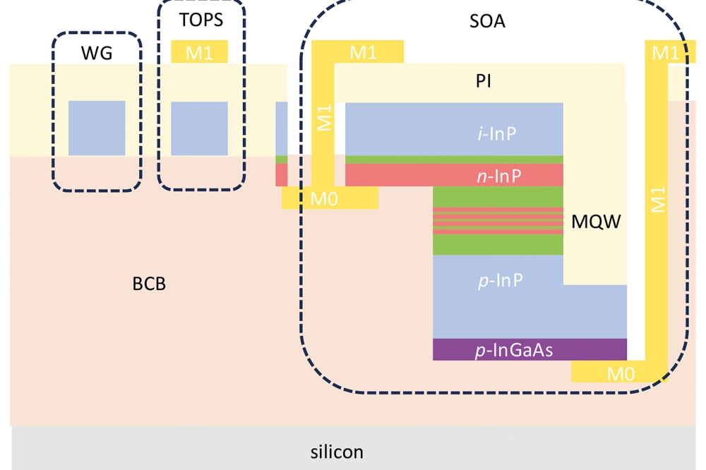
The engineers from Eindhoven have fabricated their laser with a double-sided process that realises active and passive components simultaneously. The active part is a ‘S-cross-section’ semiconductor optical amplifier, which has its two sidewalls etched on different sides of the membrane (see Figure). Metallisation of this amplifier takes place before bonding, with metal pads opened by wet etching. This is undertaken after wafer flipping and bonding to the silicon wafer with the polymer BCB.
With this design, the active-passive transition comes from evanescent coupling between the core and the intrinsically doped InP, assisted by tapering the semiconductor optical amplifier and the core.
Fabrication of passive components, including the waveguide, multi-mode interferometer, photonic crystal reflector, grating coupler and thermo-optic phase shifters, proceeds after wafer bonding, to yield a cross-sectional structure that resembles that of silicon-on-insulator photonics.
The final steps of the fabrication process are etching 120 nm-deep into the intrinsically doped InP layer to realise grating couplers, planarisation of the wafer using polyimide, and the addition of electrical contacts.
Measurements on the tuneable laser from the University of Eindhoven reveal robust side-mode operation with a maximum side-mode suppression ratio of 44 dB and a tuning range of 40 nm that spans 1555 nm to 1595 nm and encompasses critical sections of the C and L communications bands. Threshold current is 29 mA and maximum on-chip output power just over 2 mW.
The researchers says that their laser is a promising source for gas sensing applications, due to the delivery of stable emission at wavelengths corresponding to the absorption spectra of acetylene, carbon dioxide and methane.
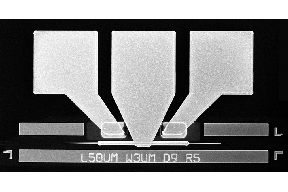
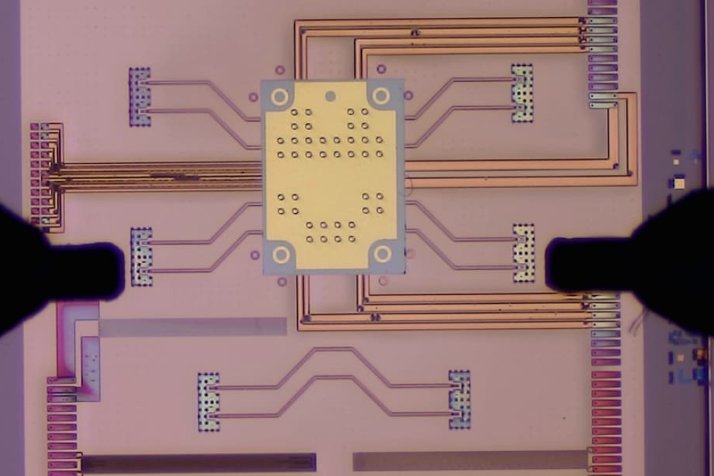
Pictured above: The photonic integrated circuit technology developed at the Eindhoven University incorporates waveguides (WG), a thermo-optic phase shifter (TOPS), and a semiconductor optical amplifier (SOA).
Reference
T. Kabir et al. Appl. Phys. Lett. 125 121110 (2024)


