IBM unveils co-packaged optics technology for AI and datacentres

The company says its innovation could boost bandwidth between chips by up to 80 times, enabling a more than fivefold reduction in energy consumption and reducing training time for a standard LLM from three months to three weeks
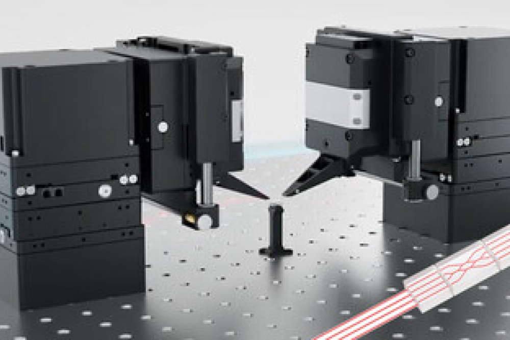
IBM has reported breakthrough research in optics technology that could dramatically improve how datacentres train and run generative AI models. Scientists at the company have developed a new process for co-packaged optics (CPO), the next generation of optics technology, to enable connectivity within datacentres at the speed of light through optics to complement existing short reach electrical wires. By designing and assembling the first publicly announced successful polymer optical waveguide (PWG) to power this technology, IBM says its researchers have shown how CPO will redefine the way the computing industry transmits high-bandwidth data between chips, circuit boards, and servers.
Today, fibre optic technology carries data at high speeds across long distances, managing nearly all the world's commerce and communications traffic with light instead of electricity. Although datacentres use fibre optics for their external communications networks, racks in datacentres still predominantly run communications on copper-based electrical wires. These wires connect GPU accelerators that may spend more than half of their time idle, waiting for data from other devices in a large, distributed training process which can incur significant expense and energy.
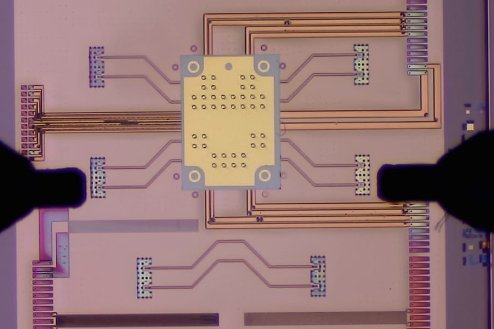
In a technical paper, IBM introduces a new CPO prototype module that can enable high-speed optical connectivity, offering a way to bring optics’ speed and capacity inside datacentres. This technology could significantly increase the bandwidth of datacentre communications, minimising GPU downtime while drastically accelerating AI processing.
According to IBM, this research innovation would enable lower costs for scaling generative AI through a more than fivefold power reduction in energy consumption compared to mid-range electrical interconnects. Another advantage of the CPO technology is up to five times faster AI model training than with conventional electrical wiring, potentially reducing the time it takes to train a standard LLM from three months to three weeks, the company says. The technique also has the potential to dramatically increased energy efficiency for datacentres, saving the energy equivalent of 5000 US homes’ annual power consumption per AI model trained.
“As generative AI demands more energy and processing power, the datacentre must evolve – and co-packaged optics can make these datacentres future-proof,” said Dario Gil, SVP and director of research at IBM. “With this breakthrough, tomorrow’s chips will communicate much like how fibre optics cables carry data in and out of datacentres, ushering in a new era of faster, more sustainable communications that can handle the AI workloads of the future.”
80 times higher bandwidth
In recent years, advances in chip technology have densely packed transistors onto a chip; according to IBM, its 2 nm node chip technology can contain more than 50 billion transistors. CPO technology aims to scale the interconnection density between accelerators by enabling chipmakers to add optical pathways connecting chips on an electronic module beyond the limits of today’s electrical pathways. IBM’s paper outlines how these new high bandwidth density optical structures, coupled with transmitting multiple wavelengths per optical channel, have the potential to boost bandwidth between chips as much as 80 times compared to electrical connections.
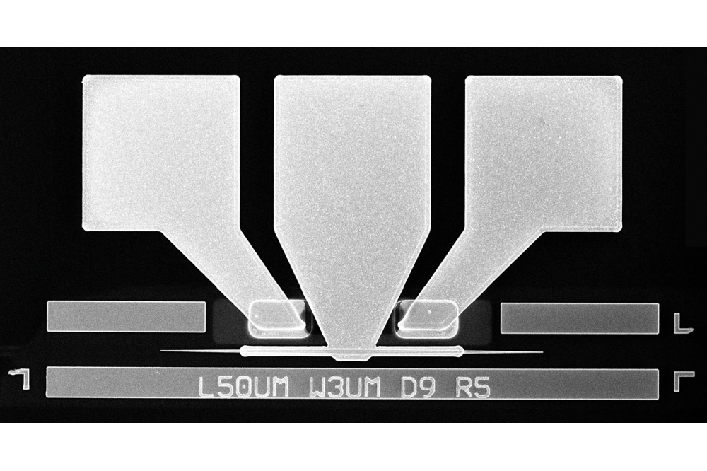
IBM’s innovation, as described, would enable chipmakers to add six times as many optical fibres at the edge of a silicon photonics chip, called “beachfront density,” compared to the current state-of-the-art CPO technology. Each fibre, about three times the width of a human hair, could span centimetres to hundreds of metres in length and transmit terabits of data per second. The IBM team assembled a high-density PWG at 50 µm pitch optical channels, adiabatically coupled to silicon photonics waveguides, using standard assembly packaging processes. The paper additionally indicates that these CPO modules with PWG at 50 µm pitch are the first to pass all stress tests required for manufacturing.


