Printing high-speed modulators on SOI
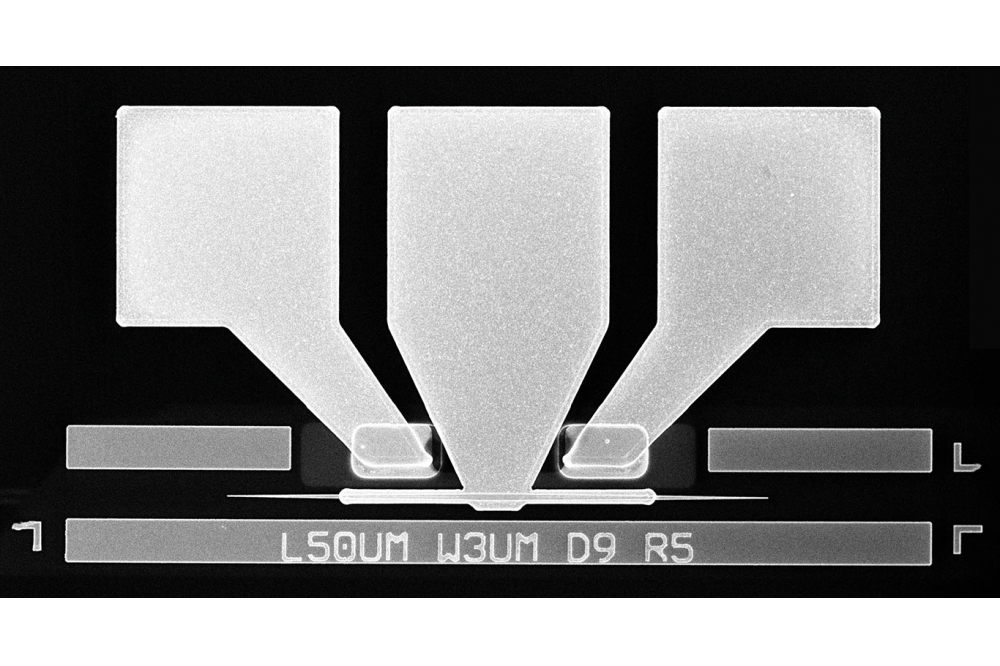
A team from the Tyndall National Institute, Ireland, is claiming to have provided the first demonstration of a micro-transfer printed electro-absorption modulator.
Their InP-based modulator, mounted to a silicon-on-insulator platform, is said to be suitable for applications in high-speed communication and sensing.
Both of the two leading forms of modulator – those based on a Mach-Zehnder interferometer and electro-absorption – combine a high bandwidth with a large extinction ratio, a low power consumption and a low operating voltage. However, the electro-absorption modulator has the key advantage of a very compact footprint.
For photonic integrated circuits, the predominant platform, in terms of materials, is silicon-on-insulator (SOI). Its merits include a high refractive-index-contrast that aids waveguiding, and the opportunity to employ mature, high-volume, high-yield, low-cost production processes. However, the indirect bandgap of SOI leads to a relative weak carrier-induced refractive index change, so it is better to produce modulators from III-Vs, such as InP.
Previous efforts by other teams have employed wafer bonding to unite InP-based modulators with SOI. However, the team from Tyndall claims that there are several advantages of replacing wafer bonding with pick-and-place techniques, such as micro-transfer printing, for uniting InP-based modulators and photonic integrated circuits based on SOI. Benefits include a potential increase in throughout, realising lower production costs through utilisation of all the devices on the source wafer, and opportunities to reuse the InP substrate and co-integrate materials through back-end-of-line processing.
The researchers have demonstrated the capability of their micro-transfer printing technology for optoelectronic circuits by transferring structures with an 80 µm by 500 µm footprint, featuring a waveguide ranging from 220 µm to 300 µm, to a 220 nm SOI waveguide circuit.
To enable the transfer of the modulator, they grow this structure, featuring a thin n-type cladding to ensure efficient coupling to the SOI waveguide, on top of InGaAs and AlInAs release layers.
Additional features of the epitaxial stack used for fabricating the electro-absorption modulator include: a small junction capacitance, to support high-speed operation; graded confinement on the p-side to enhance hole transport; and a thick confinement layer of AlInGaAs on the n-side to compensate for electron and hole transit times.
Evanescent coupling between the modulator and waveguides is realised by directly printing part-fabricated modulators on top of SOI waveguides. Tapers, increased up to 1 µm to ease the alignment placement tolerance, couple a fundamental mode from the SOI circuit to the modulator.
Production of the electro-absorption modulator from the printed coupon involves five lithographic levels, with the ridge waveguide defined using electron-beam lithography.
To assess the performance of the modulators, the team coupled light into the SOI circuit using cleaved single-mode fibres and a tuneable laser source. Measurements reveal an extinction ratio of 30 dB at 1550 nm, an electrical bandwidth of up to 40 GHz, and open-eye diagrams of up to 50 Gbit/s, using a back-to-back measurement.
“50 Gbit/s doesn’t beat any records for data transmission rates of optical modulators,” admits corresponding author Owen Moynihan. However, he argues that with the introduction of travelling-wave electrical contacts and a move to arrays of modulators, it is possible to realise far higher data rates. He points out that with this approach, there are already reports of 250 Gbit/s arrays.
Adopting this approach is one of the next goals for the team. “But more importantly, we will focus on the integration of multiple transfer printed devices, such as a laser, modulator and detector on the same chip,” says Moynihan.
Pictured above: A top view of the electro-absorption modulator, micro-transfer printed to an SOI wafer.
Reference
O. Moynihan et al. Appl. Phys. Lett 125 051102 (2024)


