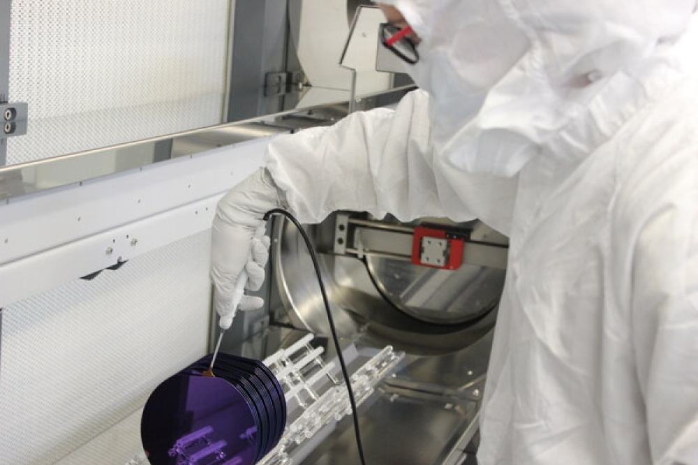
Southwest Advanced Prototyping Hub awarded $21.3 million CHIPS Act funding

The investment will support projects at Arizona State University, which leads the SWAP Hub, and at Sandia National Laboratories, a partner in the hub, in research areas including integrated photonics
The Southwest Advanced Prototyping (SWAP) Hub, led by Arizona State University, has been awarded $21.3 million in Year 2 funding under the CHIPS and Science Act to continue its work advancing America’s microelectronics industry. Arizona State University (ASU) will receive $18.6 million, with an additional $2.7 million going to Sandia National Laboratories, a lead partner in the SWAP Hub.
“This award continues the work of the SWAP Hub into its second year. We are very proud of the project awards the SWAP Hub received in Year 1 and the significant impact each area of our work is having,” said Sally Morton, executive vice president of ASU’s Knowledge Enterprise. “These initiatives highlight Arizona State University’s dedication to discovery and innovation.”
ASU's Jason Conrad, the chief operating officer for the SWAP Hub, said: “This is a vote of confidence in the work of more than 170 partners who have come together and collaborated to help build the infrastructure, connect the talent and leverage the resources to deliver results on projects that will advance the semiconductor manufacturing industry in the United States.
“The combined capabilities of the SWAP Hub network create opportunities for industry to work together to better serve the country’s national strategic objectives. This investment helps to ensure that the work continues, including projects that take advantage of SWAP Hub capabilities but are funded solely by the private sector.”
Sandia National Laboratories, a Federally Funded Research and Development Center (FFRDC) that plays a lead role in SWAP Hub operations and projects, received a specific allocation as part of the award.
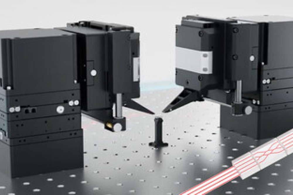
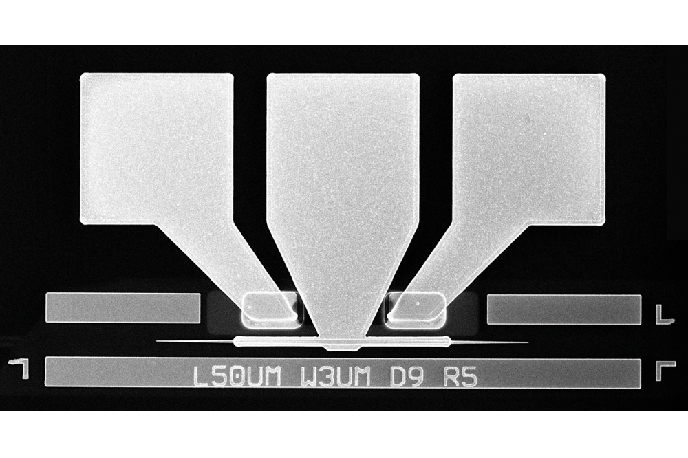
“Sandia National Laboratories is proud to partner with the SWAP Hub to enhance the regional microelectronics ecosystem,” said Ken Dean, Sandia’s senior manager of advanced semiconductor technologies. “Our expertise in national security microelectronics and our extensive fabrication capabilities will support the transition of advanced technologies from the lab to fab to production. This Department of Defense Microelectronics Commons investment will expand access to critical tools and processes for hub members, facilitating projects in CMOS+X integration, power electronics, heterogeneous integration and photonic integrated circuits.
“Additionally, Sandia is coordinating workforce initiatives with ASU and SWAP Hub member universities and community colleges in Arizona, New Mexico, Utah and Colorado to train the next generation of national security semiconductor leaders.”
Headquartered in Arizona, the SWAP Hub aims to connect the large Southwest semiconductor cluster, which has more than $100 billion in private investment, to a growing network of defence and electronics partners across the country.
The SWAP Hub is one of eight regional innovation hubs established under the Department of Defense’s Microelectronics Commons, a national strategic initiative to accelerate the development and production of microelectronics technologies that are critical to US security and defence. It links semiconductor prototyping facilities at ASU’s MacroTechnology Works, Sandia National Laboratories’ Mesa Fab and NXP’s power electronics fabrication facility in new ways to produce prototypes for the Department of Defense that no single institution could develop alone.


