Miniaturised high-power amplifiers for optical microchips

Researchers have reported a new millimetre-sized amplifier with an output of more than 1 watt, a step that they say will make it easier to use integrated photonics devices in surgery, sensing, and future accelerator systems and X-ray sources
Researchers at DESY have reported developing a millimetre-sized high-power amplifier with an output power of more than one watt on silicon-based optical microchips. According to the team, this output power is many times higher than what was previously achievable on this tiny scale and enables the use of high-power on-chip amplifiers in the field of integrated photonics instead of external amplifiers. The scientists say this would make it much easier and cheaper to operate miniaturised devices and sensors, such as those increasingly used in medical surgery, remote sensing by laser, and telecommunications, as well as in optical circuits for future accelerator systems and X-ray sources. The researchers have now reported in the journal Nature Photonics that they have confirmed through experiments that these very compact high-performance amplifiers are possible.
High-power amplifiers are critical components in modern optical systems. “In order to be able to use them more widely, such systems should be very small, analogous to microelectronics – preferably in the millimetre range – but without delivering less power. They should also be able to be mass-produced and therefore cost relatively little,” says Neetesh Singh, first author of the study, who works in the DESY group for ultrafast laser and X-ray physics at the Center for Free-Electron Laser Science (CFEL).
However, miniaturisation has its limits because the smaller an optical system is, the less energy it can store and the less power it can provide. To date, it has not been possible to build suitably small, high-performance optical amplifiers that can be integrated on a microchip. Instead, such microsystems have so far been dependent on external, much larger benchtop amplifiers.
In the new study, however, Singh's team used a so-called Large Mode Area (LMA) waveguide, which they had previously developed themselves, for the first time to amplify a light signal in a very small space. The critical factor here is the cross-sectional area of the electric field conducted by the waveguide, known as the “mode.” In the current experiments, Singh's team report successfully increasing the cross-sectional area of the mode in a photonic waveguide made of silicon nitride and aluminium oxide from just one to 30 square micrometres. This enabled the output power to be increased from a few dozen milliwatts to over one watt, the team says.
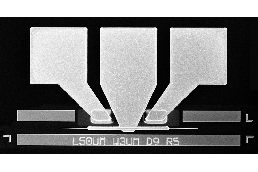
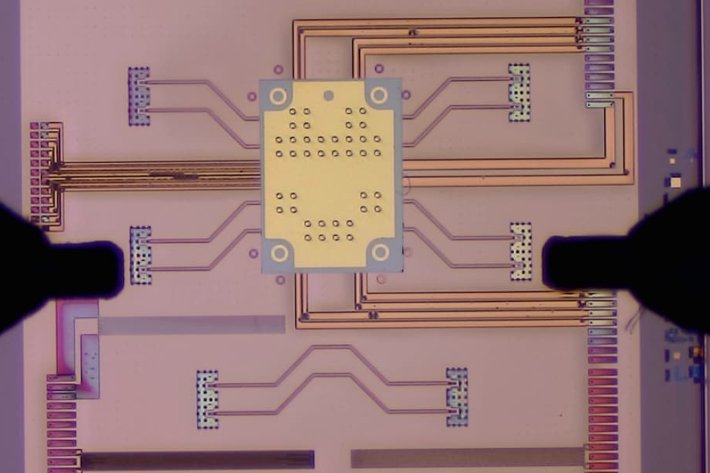
According to the researchers, these results are thanks to an ingenious design of the microchip surface, which is only four square millimetres in size and on which the light signal is sent through a narrow, embedded silicon nitride waveguide covered with an aluminium oxide layer of controlled thickness. The silicon nitride waveguide can be guided several times through a so-called LMA region. As in other photonic waveguides, the optical signal conducted in the waveguide starts out small, weak, and directly within the waveguide. However, it then passes through a specifically designed tapering of the waveguide.
“This forces the mode out of the waveguide, so to speak, significantly increasing its cross-section and allowing it to float like a cloud through the aluminium oxide layer above the waveguide,” explains Singh. “However, it remains connected to the original waveguide as a lead, like a hot air balloon to its basket.” The aluminium oxide layer is full of thulium ions, which are put into an excited, high-energy, state by a so-called optical pump – an external laser. The signal photons of the mode now interact with these ions in a comparatively large area, which is referred to as the “Large Mode Area” or “LMA area.” And precisely because the mode is now so large, the photons can interact with a large number of energetic ions and extract energy from them. “Just as a large snowplow can sweep more snow at once than a small snow shovel, a large mode can contain more ions,” says Singh.
The researchers amplify the signal even further by sending it through the LMA area several times. To do this, the waveguide expands again, drawing the signal cloud floating above it back into the narrow silicon nitride waveguide, making a 180-degree turn at the edge of the chip, passing the signal through the LMA area again and tapering off once more, so that the mode is pressed into the high-energy layer again in order to absorb even more power.
In the end, the researchers say, you get a much stronger signal than at the beginning, in the smallest possible space, integrated on a microchip, and the quality of the signal is retained. With this technology, external amplifiers will no longer be necessary in many systems, making the systems not only smaller, but also cheaper and more reliable.
“Our micro LMA high-power amplifier will allow us to integrate complex optical circuits with high output power in the future, as we have long known from microelectronics,” emphasises Franz Kärtner, head of the group for ultrafast laser and X-ray physics, who also teaches as a professor of physics at the University of Hamburg. “This will allow us to produce complex optical systems for accelerators, X-ray sources, or many other applications at low cost and with high reliability.”


