High Tech Campus Eindhoven invests in facilities for TNO’s 6-Inch photonic chip pilot line

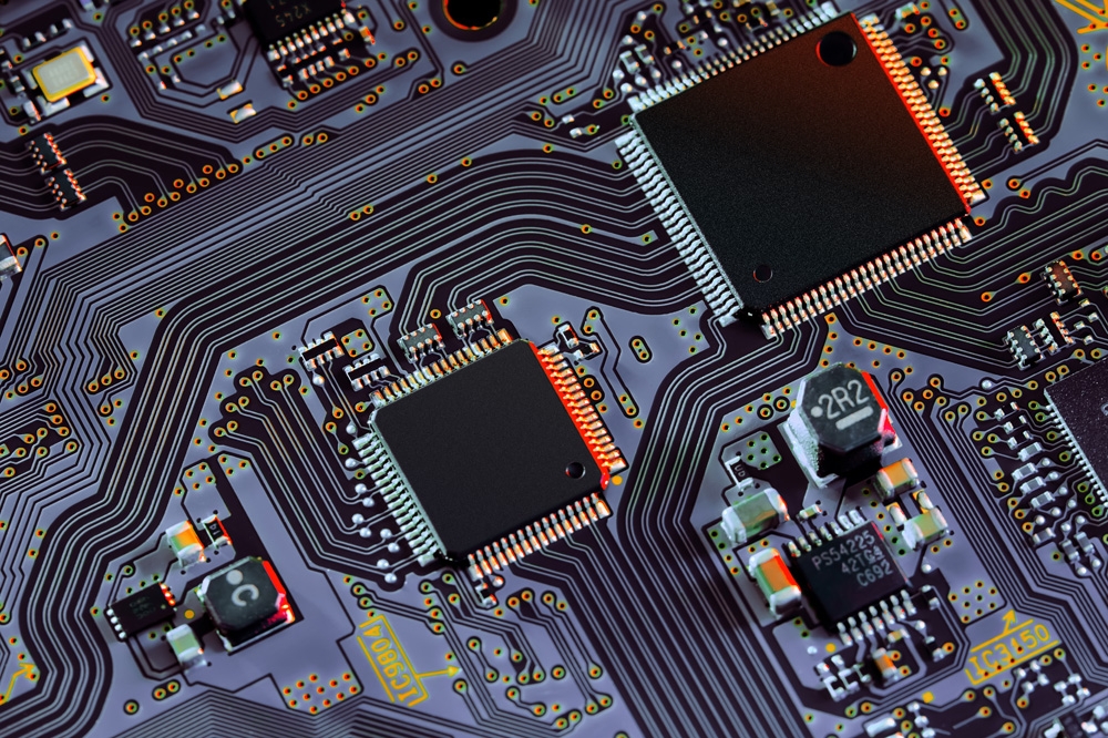
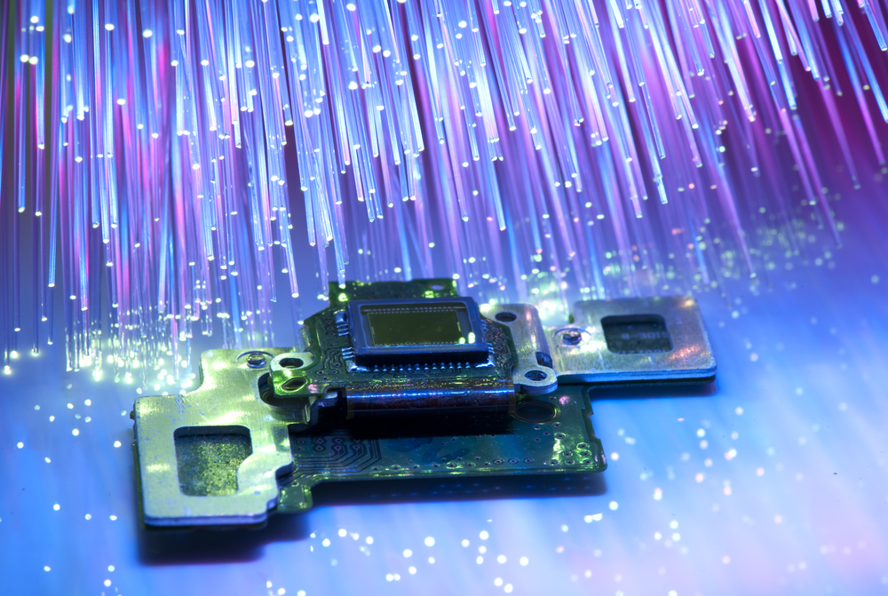
High Tech Campus Eindhoven (HTCE) will host a new industrial pilot line for photonic chips, developed by TNO as part of the EU’s PIXEurope project. Construction of the building and cleanroom facilities will begin in February 2026 on the north side of the campus. Once operational, the facility will serve as both a testbed and fabrication site for advanced Indium Phosphide (InP) photonic chips, enabling full-scale manufacturing at a 6-inch wafer level.
The new pilot line represents a major step toward industrial-scale photonic chip production in the Netherlands and Europe. By combining research and manufacturing capabilities, the facility aims to accelerate the transition from innovative ideas to energy-efficient and reliable real-world technologies. With a capacity to produce up to 10,000 wafers per year, it will significantly increase throughput and efficiency for integrated photonic devices.
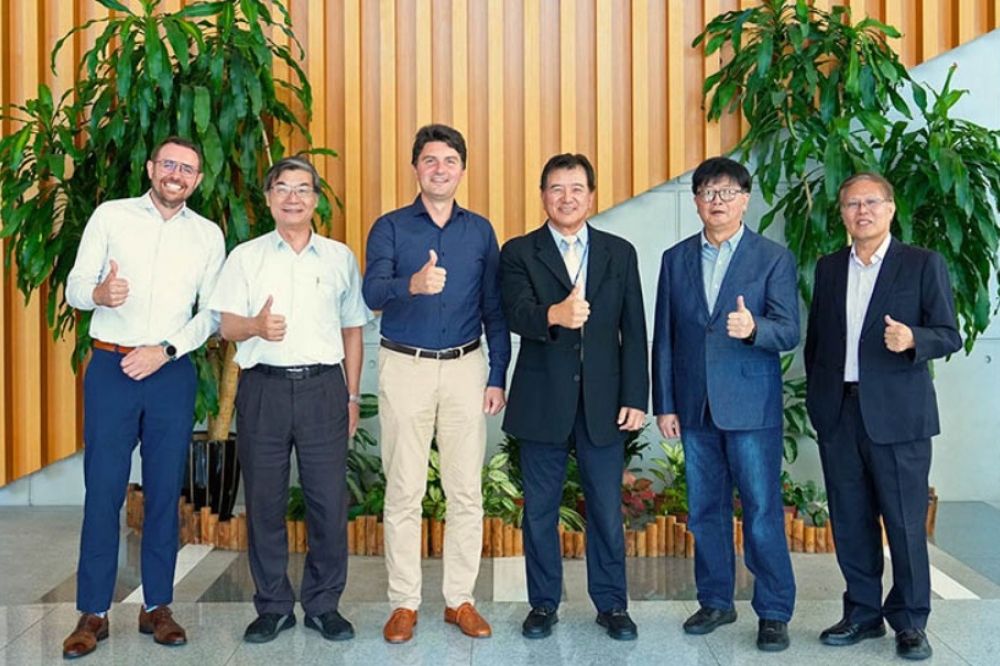
Ton van Mol, Managing Director at TNO, described the initiative as a game-changer for Dutch companies and a key part of the PhotonDelta ecosystem that positions the Netherlands as a leader in photonics. Otto van den Boogaard, CEO of HTCE, said the campus is proud to invest in and provide the facilities for the pilot line, reinforcing its role as a hub for breakthrough technology and innovation.
HTCE’s investment reflects its commitment to projects that strengthen the region’s technological ecosystem and national earning capacity. The collaboration between TNO, PhotonDelta, and HTCE underlines the importance of local infrastructure in scaling up Europe’s photonics manufacturing capabilities and supporting the growth of the integrated photonics industry.