Ennostar and X-Celeprint collaborate on silicon photonics integration

By combining Ennostar’s production capabilities in high-volume optoelectronics and micro-scale devices with X-Celeprint’s expertise in micro-transfer printing, the companies aim to achieve performance breakthroughs and accelerate volume production of silicon photonics across several industries
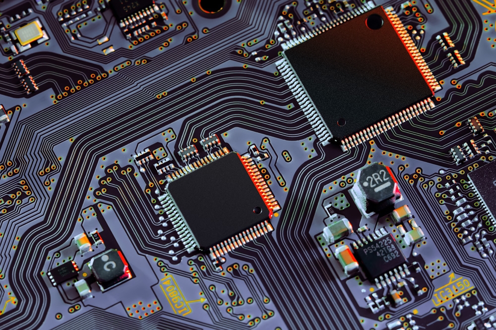
Ennostar, a provider of optoelectronic semiconductors, has announced it is partnering with X-Celeprint, a company specialising in micro-transfer printing (MTP) technology, to accelerate the adoption and commercialisation of mass transfer technology in silicon photonics.
Ennostar says it brings expertise in high-volume optoelectronics manufacturing and micro-scale devices such as micro LEDs, while X-Celeprint contributes know-how in MTP for heterogeneous integration that will enable efficient, scalable, and production-ready silicon photonics solutions.
“Our focus is to drive innovation in AI optical interconnects, including solutions based on micro LED, VCSEL, and CW-DFB LD technologies,” said Patrick Fan, chairman of Ennostar Corporation. “By combining Ennostar’s advanced manufacturing know-how with X-Celeprint’s world-leading MTP technology, we believe this collaboration will play a pivotal role in the silicon photonics ecosystem. Through heterogeneous integration, we aim to unlock new breakthroughs in both performance and innovation for the next generation of photonic devices.”
Peter Smyth, CEO at X-Celeprint, added: “By working with Ennostar, we are creating a seamless path for companies to accelerate volume production of silicon photonics across multiple industries.”
Under the planned collaboration, X-Celeprint will provide its MTP technology and support its customers in qualifying their products for MTP while Ennostar will act as a key manufacturing partner, supporting production. Both companies will jointly evaluate market opportunities and strategically engage with third parties, aiming to drive the commercialisation of advanced photonics solutions.
Ennostar notes that mass transfer technology, previously applied in micro LED displays, has already reached a level of maturity. With the rise of AI and high-performance computing, the demand for high-speed data transmission in datacentres and advanced computing systems is rapidly increasing, driving an urgent need in the optical communication industry for heterogeneous integration and high-density packaging. Compared to traditional processes, Ennostar says that MTP offers significantly greater efficiency and precision, making it a key enabler to meet the challenges of next-generation industry upgrades.
“The introduction of MTP can increase transfer speeds by more than 30 times compared with conventional processes while also improving transfer accuracy by 85 percent,” said CN Huang, vice president of Ennostar’s Advanced Research Center. This represents a significant breakthrough in the integration of semiconductors and optoelectronic components for co-packaged optics (CPO).
Looking ahead, Ennostar plans to continue to deepen its technology partnerships and expand market opportunities, working closely with ecosystem partners to advance silicon photonics technologies and deliver competitive integrated solutions.