CORNERSTONE installs advanced E-beam lithography systems
Unveiled by the UK’s science minister this week, the new equipment aims to support the foundry’s mission to accelerate the commercialisation of silicon photonics technologies by providing researchers and industry with access to world-class nanofabrication resources
CORNERSTONE Photonics Innovation Centre (C-PIC), the UK’s dedicated Innovation and Knowledge Centre (IKC) for silicon photonics innovation, has announced the installation of new state-of-the-art electron beam lithography (E-beam) systems, further expanding its services.
C-PIC says the addition of this equipment marks a pivotal step for the CORNERSTONE foundry, helping to foster the development of high-precision silicon photonics and enable a faster transition from research into scalable, market-ready solutions.
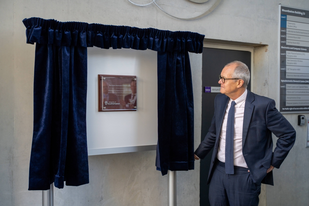
The new facility was officially opened by the UK's science minister, Patrick Vallance, during a recent visit to the University of Southampton. He was joined by Mark E. Smith, vice-chancellor of the University of Southampton, Graham Reed, head of the Optoelectronics Research Centre and CORNERSTONE, and Osamu Wakimoto, managing executive officer at the Japan Electron Optics Laboratory (JEOL).
“Britain is home to some of the most exciting semiconductor research anywhere in the world – and Southampton’s new E-beam facility is a major boost to our national capabilities,” said Vallance. “By investing in both infrastructure and talent, we’re giving our researchers and innovators the support they need to develop next-generation chips right here in the UK.”
Vallance also outlined wider UK investment designed to accelerate technological innovation, adding: “Our £4.75 million skills package will support our Plan for Change by helping more young people into high-value semiconductors careers, closing skills gaps and backing growth in this critical sector.”
Reed commented: “The introduction of the new E-beam facility will reinforce our position of hosting the most advanced cleanroom in UK academia. It facilitates a vast array of innovative and industrially relevant research, and much-needed semiconductor skills training.”
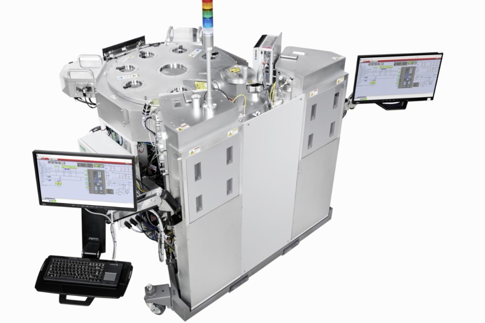
According to CORNERSTONE, the new equipment from JEOL – a global supplier of scientific and metrology instruments – includes several state-of-the-art systems, some of which are the first installations outside Japan.
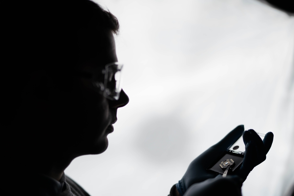
E-beam lithography is essential for fabricating nanoscale photonic and electronic components that power next-generation applications. The newly installed JBX-8100FS 200 kV equipment offers high-resolution and high-throughput exposure modes, facilitating diverse patterning applications and ultrafine processing for small- to medium-scale production.
The C-PIC says these landmark additions enable ultra-high-resolution patterning critical for pushing the frontiers of silicon photonics device development. With the enhanced performance offered by the new JEOL systems, the CORNERSTONE foundry aims to more closely emulate manufacturing operations seen in high-volume silicon photonics fabrication facilities, thus helping to remove challenges that can occur when scaling silicon photonics designs.