Project RAMPLAS paves the inroad for Optical RAMs and Optical Cache Memories

The research project Ramplas, "100 Gbps Optical RAM on-chip: Silicon-based, integrated Optical RAM enabling High-Speed Applications in Computing and Communications", funded in part by the European Commission under ICT-FET Open, completed successfully its activities delivering the most basic building blocks towards high-speed optical RAMs and optical cache memories.
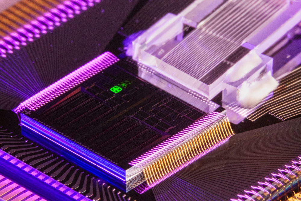
RAMPLAS managed to deliver a number of breakthroughs that set the most basic cornerstones towards low-energy and high-speed integrated optical RAM and optical cache memory solutions. RAMPLAS was conceived almost 5 years ago upon the need to investigate optical memory technologies as an alternative for addressing the steadily increasing gap between processor and memory speed that is commonly referred to as the "Memory Wall". Working towards its goals, the RAMPLAS consortium established the theory fundamentals for optical RAMs confirming their potential to perform >10x faster than electronic RAMs, advancing at the same time Semiconductor Optical Amplifier (SOA) modelling towards allowing reliable optical memory simulations. It also demonstrated successful optical RAM as integrated chip using three different technology platforms (silicon photonics, InP monolithic and InP-on-Si photonic crystals) and paving the way towards energy-efficient and miniaturized optical RAMs. Moreover, RAMPLAS produced the first "blue-print" design of a practical optical cache memory performing 5x faster than current electronic caches. Besides the elementary optical RAM cells, RAMPLAS demonstrated experimentally all relevant building blocks required for a complete optical cache like optical Row/Column Decoders and optical Tag Comparison circuits. Last but not least, RAMPLAS highlighted the benefits of an optical cache memory when employed in current computational settings, allowing for a relaxed memory hierarchy while offering significant speed-up for a broad range of workloads. In these efforts, RAMPLAS consortium worked out technological solutions that can be of benefit to a wider range of applications: It delivered the first optical Content Addressable Memory (CAM) cell as an integrated chip, laying down new perspectives in address look-up routing applications. At the same time, photonic integration technologies witnessed significant progress in the areas of dilute nitride SOAs and Silicon Photonics, rendering their use as a promising alternative towards high-speed, energy-efficient and practical chip-scale fabrication platforms for optical interconnects and for optical access network applications.
The consortium was headed by the Centre for Research and Technology Hellas, CERTH, (Greece, the photonics teams leading RAMPLAS technical work recently moved to the Aristotle University of Thessaloniki, AUTH, joining AUTH's Center for Interdisciplinary Research and Innovation, CIRI) and comprised the Technical University of Berlin (Germany), VTT (Finland), PhoeniX Software (the Netherlands), Institute of Communication and Computer Science, ICCS, (Greece) and the Tampere University of Technology (Finland). More information about the project goals and highlights can be found on youtube and in on its website www.ict-ramplas.eu.


