Fraunhofer IMS invites participation in PIC engineering runs
The institute has announced advanced photonic integration capabilities, with a silicon nitride-based platform supporting low-loss, broad-wavelength applications
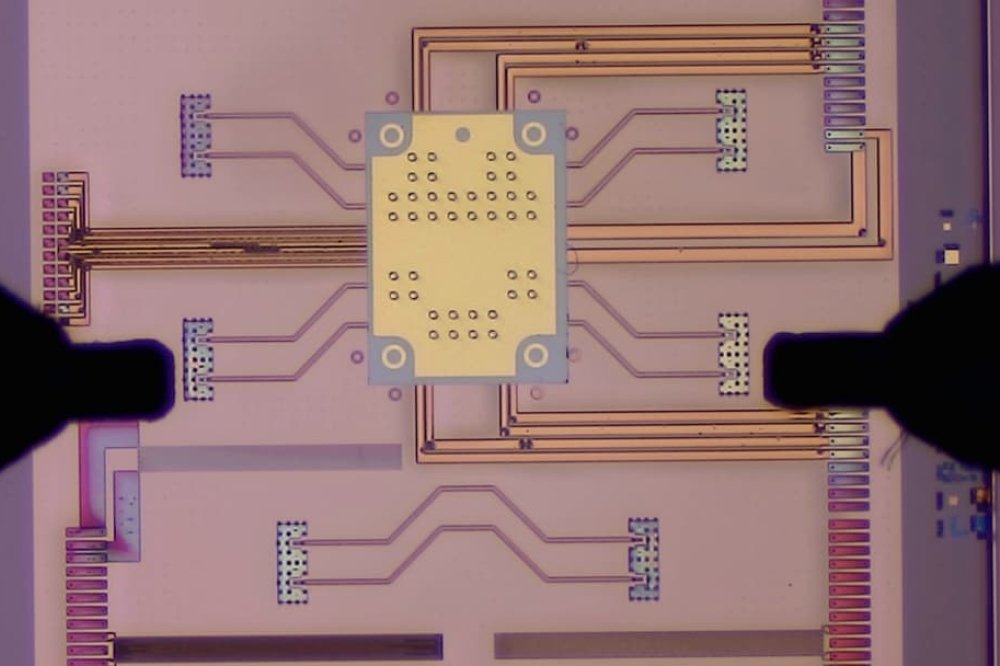
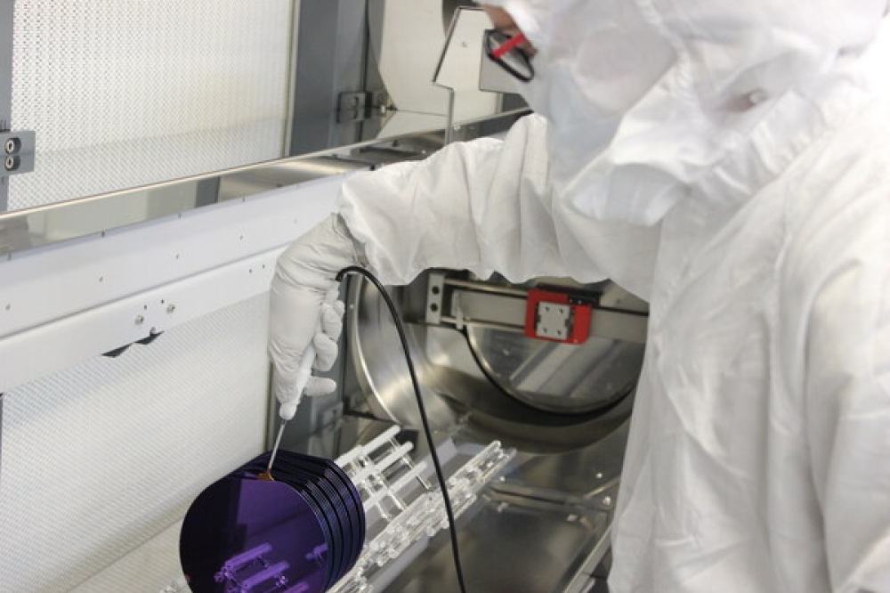
Fraunhofer IMS, the centre for microelectronics and smart sensor systems within the Fraunhofer-Gesellschaft, has announced it has advanced capabilities in PICs on a 200 mm wafer manufacturing environment. The centre says its facilities are tailored for low-volume R&D and pilot manufacturing, ensuring flexibility and scalability for various projects.
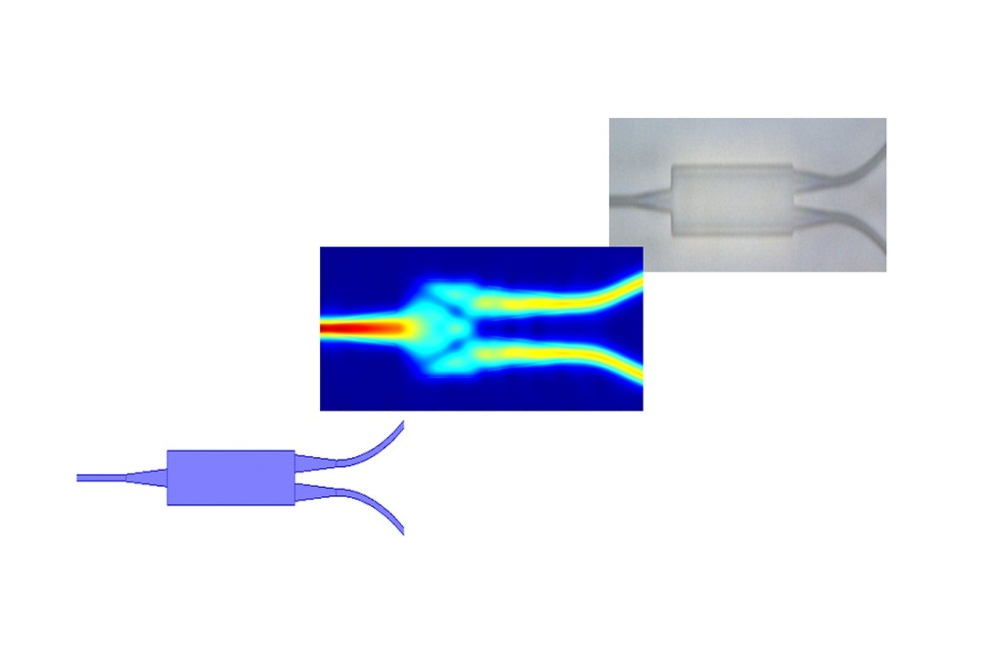
According to Fraunhofer IMS, its silicon nitride-based photonic platform is a state-of-the-art platform that supports low-loss, broad-wavelength applications. The institute adds that it is enhanced with the opportunity of novel quasi-monolithic integration, allowing for a vast range of waveguide materials, including, for example, silicon nitride and tantalum pentoxide, covering visible to mid-infrared wavelengths from 370 nm to 3 µm. Current photonic components include couplers, waveguides, and interferometers, with the option for custom designs.
Additionally, Fraunhofer IMS offers support for technology, device, and circuit simulations, considering packaging and system-level needs, and the team seeks to ensure high-quality outcomes throughout the development.
With expertise in microelectronics, micro-electromechanical systems (MEMS), and photonics, the institute focuses on post-CMOS integration of PICs for smart sensor systems. This includes working with external foundry wafers for applications in optical computing, biosensors, and on-chip quantum photonics.
Fraunhofer IMS invites participants to engage in engineering runs starting Q1 2025 to create their own PIC designs in a high-quality clean room, adding that it is an ideal opportunity for innovators looking to bring their photonic designs to life with the support of cutting-edge facilities and expertise.
Image: Fraunhofer IMS


