Integrating high-speed germanium modulators with silicon photonics and fast electronics
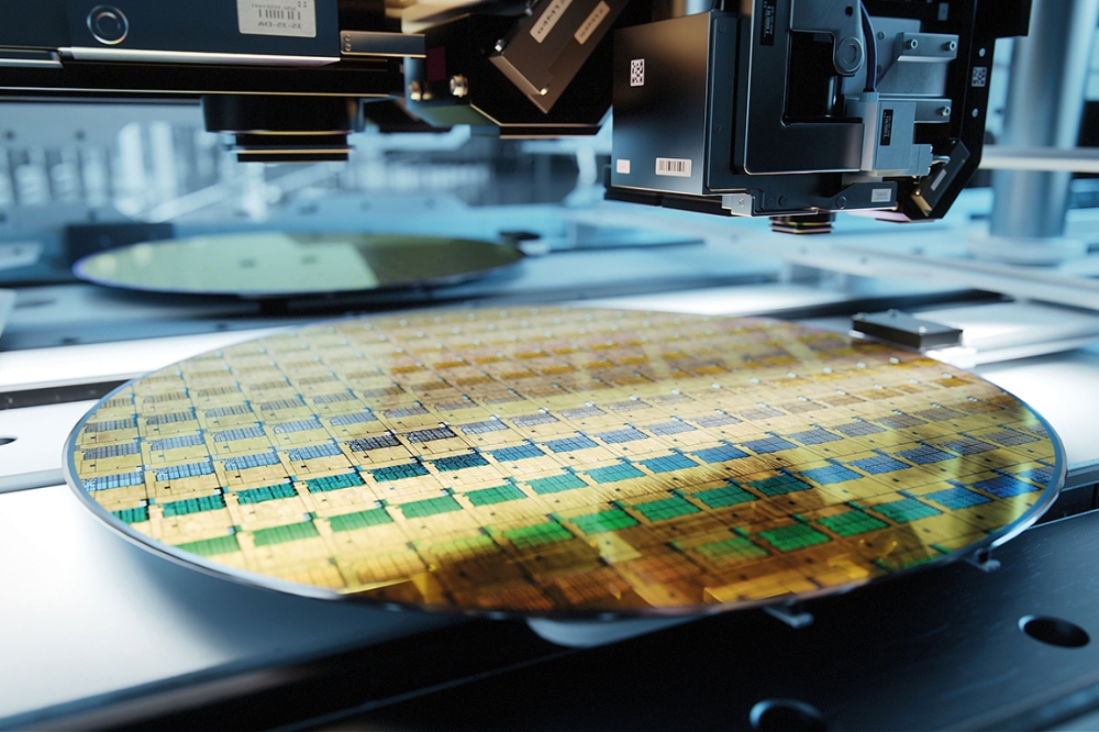
A major bottleneck in optical transmission is emerging, as silicon Mach-Zehnder modulators approach their limits. In our data-driven era, the industry urgently needs higher-bandwidth, energy-efficient modulators that are compatible with silicon photonics. Germanium electro-absorption modulators offer a promising route forwards.
By Daniel Steckler, Stefan Lischke, and Lars Zimmermann,IHP-Leibniz Institut für innovative Mikroelektronik
Optical connectivity plays a major role in all our daily lives, often without us even noticing it. Video calls, cloud storage, social media, and on-demand video and audio are all constantly at our fingertips. Artificial intelligence (AI) applications are also on the way to becoming ubiquitous everyday companions. But all of this is only possible thanks to modern datacentres. Fibre-optic communication, not only to and from datacentres, but also within them, is the key to coping with the enormous data flow these technologies generate.
According to the Ericsson Mobility Report from November 2023, global data traffic has more than doubled every two years over the past 10 years. By 2029, global mobile data traffic is projected to triple, reaching 403 exabytes per month [2]. Since every single bit transmitted consumes a certain amount of energy, the energy efficiency of optical and electrical devices is increasingly important. One hyperscale datacentre already consumes as much energy as 80,000 US households [1]. And that doesn’t even include the energy required for transport to the datacentres.
Figure 1: TEM images of germanium photodiode (a) and electro-absorption
modulator (b). Cross sections cut perpendicular to the light-incidence
direction. As indicated by the red boxes the Si-region has been reduced
from 220 nm to 100 nm for the electro-absorption modulator.
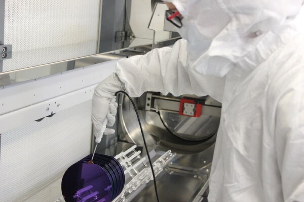
Besides energy efficiency, other demands on future devices include high-volume and low-cost fabrication capabilities and high-speed performance. Thanks to sophistic–ated fabrication processes on 200 mm and 300 mm wafers, silicon photonics has seen rapid progress, becoming a major technology in fibre-optic communication applications. In fact, silicon photonic transceivers for datacentre interconnects enabling 400 G bitrates are already available on the market and 800 G transceivers have been demonstrated.
However, while the effective data rates of transceivers have increased from 10 G in 2007 to 800 G in 2024, the rate of transmitted light pulses (symbol or baud rate) has actually only scaled by a factor of five (from 10 GBaud, in 2007 to 50 GBaud today). For this reason, techniques such as higher-order modulation or multiple lanes are deployed on a large scale to cope with the data-traffic requirements [3].
Figure 2: Schematic longitudinal cut through the EAM to visualize the butt-coupling approach (not to scale).
On the receiver side, germanium photodetectors with a 3 dB bandwidth well beyond 200 GHz have already been demonstrated [4]. However, a major bottleneck is emerging on the transmitter side. With electro-optical 3 dB bandwidths of 50-70 GHz, silicon Mach-Zehnder modulators, the most established devices in silicon photonic transmitters, seem to have reached their performance limits already. Facing the data-traffic growth projections, it is unlikely that using the aforementioned modulation formats or even more parallelisation alone will be sufficient. Achieving symbol rates beyond 100 GBaud will require extensive equalisation and digital signal processing (DSP), but this is detrimental to the system’s power efficiency. To avoid this, the industry urgently needs modulators with 3 dB bandwidths above 100 GHz.
Figure 3: Normalized frequency response of electro-absorption modulator
at wavelength of 1.6 µm at a bias of -1 V and -3 V for an optical input
power of Pin = 6 dBm at fibre tip, estimated on Keysight 110 GHz LCA.
To this end, researchers have put extensive efforts into developing alternative modulators in recent years, investigating materials such as lithium niobate, barium titanate, silicon-organic hybrid modulators, and plasmonic modulators. In 2023, for example, researchers demonstrated resonant plasmonic micro-racetrack modulators with 3 dB bandwidths of 176 GHz and symbol rates of 220 GBaud [5].
However, monolithic integration of modulators based on “exotic” materials onto silicon photonics platforms presents considerable challenges, such as CMOS cleanroom compatibility, cross-contamination, and reliability. To date, no full platform integration of such modulators has been demonstrated without significant performance losses.
Electro-absorption modulators
To overcome the bandwidth bottleneck, we need a modulator that is compatible with silicon photonics, simultaneously enables bandwidths above 100 GHz, and also allows energy-efficient optical modulation. Germanium electro-absorption modulators (EAMs) represent a very promising candidate for meeting these criteria.
Figure 4: Eye diagrams of RF-probed germanium EAM at data rates of 80,
100, and 112 Gbps. The dynamic extinction ratios are 2.9 dB (80 Gbps),
2.75 dB (100 Gbps), and 2.3 dB (112 Gbps) with four-tap linear
equalization on the receiver side. Vbias = -1.5 V and an AWG output signal of 2.3 Vpp.
For this purpose, we can use a device with a structure very similar to a photodiode. While the latter is located at the end of an optical waveguide (where the incident light is converted into photocurrent), the modulator is intended to change the intensity of the light, by either absorbing or transmitting it. For transmission, the incoming light must not be absorbed, which limits the usable wavelengths to the range where germanium no longer absorbs. This happens in the range of 1.6 µm and beyond.
However, we can significantly enhance the optical absorption of germanium in this wavelength range with the application of an electric field – a phenomenon known as the Franz-Keldysh effect. In other words, we can use an electric field to change the optical absorption of a semiconductor – hence the term electro-absorption modulators (EAMs).
The Franz-Keldysh effect is intrinsically a very fast process and theoretically enables modulation in the THz regime. However, the EAM itself is limited by the time it takes for the electric field to build up, which is governed by the resistance and capacitance of the device.
Figure 5: Normalized frequency response of germanium photodiode at a wavelength of 1.6 µm for optical input power of Pin = 0 dBm at fibre tip, estimated on Keysight 110-GHz lightwave component analyzer (LCA).
In 2007, MIT scientists demonstrated the first waveguide-coupled germanium EAM with a 3 dB bandwidth of around 1 GHz [6]. Since then, a lot of research has gone into increasing the performance of these devices. In 2023, the National Information Optoelectronics Innovation Center in Wuhan, China, demonstrated a germanium EAM with a 3 dB bandwidth higher than 110 GHz [7].
IHP’s silicon-germanium BiCMOS technology
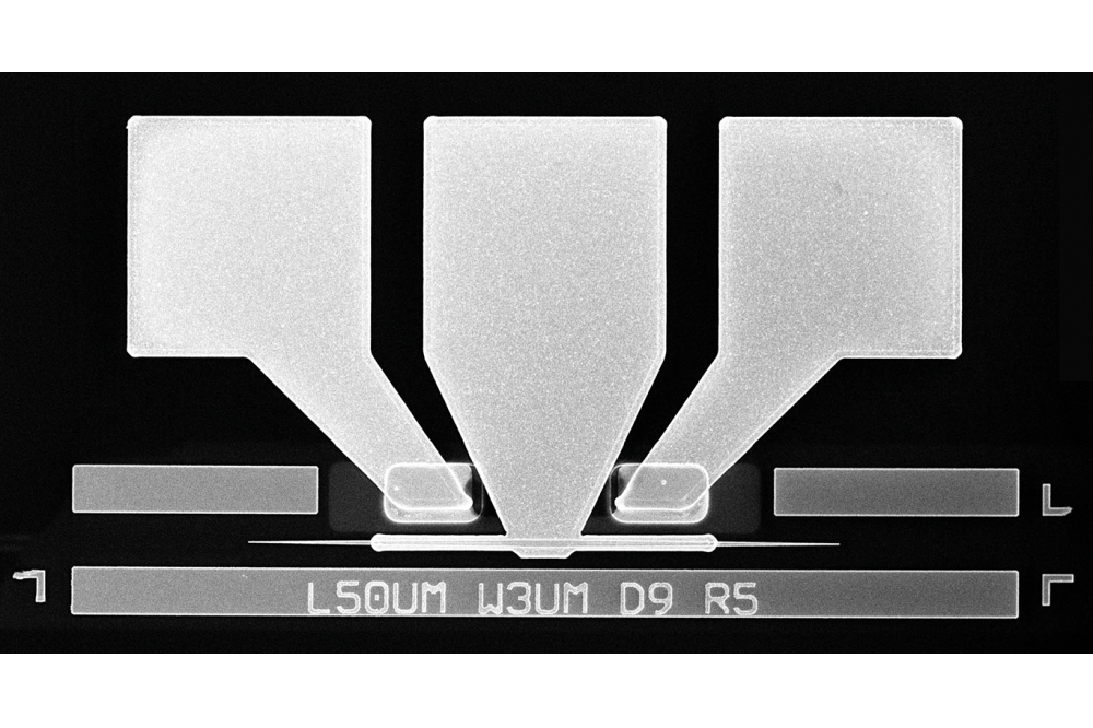
At IHP, we are aiming to develop and improve germanium EAMs with 3 dB bandwidth of at least 100 GHz to be further integrated into our unique photonic silicon-germanium BiCMOS technology platform [8], a process that enables electronic PICs (ePICs).
This innovation monolithically combines photonic devices such as optical waveguides, phase shifters and high-speed germanium photodiodes with CMOS transistors and high-performance silicon-germanium heterojunction-bipolar transistors (HBT) on the same wafer substrates. This benefits RF performance significantly while simultaneously reducing packaging and assembly efforts.
In 2023, we demonstrated the first >100 GHz germanium EAM monolithically integrated along with germanium photodiodes with 3 dB bandwidth of 80 GHz. Indeed, both of these devices were integrated into the aforementioned photonic BiCMOS technology platform, i.e. together with CMOS and silicon-germanium HBT [9].
Figure 6: Box-plots of unity gain frequency fT and of maximum oscillation frequency fmax measured on 13 wafers from one lot, 9 chips measured on each wa
IHP’s germanium EAM device scheme is in general very similar to that of the photodetector. However, the requirements on the coupling between the silicon waveguide and the germanium are different, because absorption must happen for photodetection, whereas an EAM must perform amplitude modulation.
In the latter case, coupling is far more critical, since the optical mode should pass through the device with the lowest possible loss when the device is in the off state (when it is supposed to be “transparent”). Therefore, it is essential to maximise the overlap between the optical modes of the silicon waveguide and the germanium region of the EAM. We can achieve this by locally reducing the silicon thickness below that of the germanium.
In our technique, we were able to realise this without additional processes or mask efforts, by utilising the silicon dry etch originally applied to form rib waveguides for silicon Mach-Zehnder modulator phase shifters.
Table 1: Overview of state-of the art Si-based modulators available in
recent silicon photonics platforms. We compare Mach-Zehnder modulators
(MZM) to resonant ring modulators (RRM) and electro-absorption
modulators (EAM) as more compact device alternatives. Definition of the
optical windows: O-band: 1260-1360 nm, C-band: 1530-1565 nm, L-band:
1565-1625 nm.
High-speed results
Our germanium EAMs exhibit excellent RF performance with a 3 dB bandwidth of 100 GHz at -3 V bias. These devices’ high-speed performance yields clearly opened eye diagrams at a data rate of 112 G. Figures 3 and 4 show the frequency response of the EAM and the eye diagrams, respectively.
The dynamic power consumption can be calculated by ∆Ebit = CVpp2/4, where C is the junction capacitance and Vpp is the modulation voltage. With C = 7.5 femtofarad and Vpp = 1.8 V, the dynamic power consumption is estimated to be 6.08 femtojoules per bit, which is a peak value amongst the silicon photonics-based modulators published to date.
In particular, the Franz-Keldysh effect enables efficient absorption in the wavelength range in which germanium otherwise absorbs only poorly. At λ = 1.6 µm, the co-integrated germanium photodiodes yield reasonably high internal responsivities of 0.33 A/W at -2 V and 0.45 A/W at -4 V bias. Simultaneously, the photodiodes exhibit 3 dB bandwidth of 80 GHz, determined at the same wavelength, as shown in Figure 5. Thus, the photodiode complements the fast modulators, which is crucial for monolithic integrated transceiver systems.
Importantly, integrating EAMs did not reduce the performance and yield of the electronic components such as 0.25 µm CMOS transistors and silicon-germanium HBTs. Figure 6 demonstrates the high-frequency behaviour of the latter, showing cut-off frequencies fT and fmax of ~240 GHz and ~280 GHz, enabling high-speed modulator driver or transimpedance amplifier circuits.
Table 1 compares various silicon photonics platforms by means of their modulator performance to benchmark our results. In comparison with the other modulators, our ePIC-integrated EAM exhibits outstanding performance in terms of energy efficiency and electro-optical bandwidth.
These characteristics will pave the way for the design of small-footprint transmitters for >100 GBaud data-rate applications to cope with future data-traffic requirements.
Outlook
To date, our EAM has demonstrated promising results at wavelengths within the L-band (around 1610 nm). For a broader range of applications, however, operation within the C-band (1530-1565 nm) is favoured due to its widespread use in telecommunications.
This can be addressed by fine-tuning the absorption characteristics through the incorporation of silicon into the germanium. Researchers at MIT and imec have previously demonstrated that a silicon content in the range of about 1 percent shifts the absorption into the desired wavelength region.
We aim to further identify and overcome current bandwidth limitations in order to optimise the germanium EAMs towards 3 dB bandwidths well beyond 100 GHz, pushing the boundaries of what is currently achievable.


