HieFo indium phosphide fab resumes production

The company says the photonic devices produced at the facility in Alhambra, California, have passed reliability validation testing, and include a new chip design that can support 1.6T single-carrier wavelength transceivers
HieFo Corporation, a US-based manufacturer of photonic devices for the optical communications and sensing industries, has announced that its indium phosphide (InP) wafer fab facility located in Alhambra, California, resumed production on 23 August 2024.
HieFo was established with the recent management buyout of wafer fab and chip-related assets from EMCORE Corporation. The company acquired the assets and started operations in early May 2024. By acquiring these assets and hiring original key scientists, engineers, and the operations team, HieFo says it has inherited more than four decades of best-in-class InP chip design, manufacturing expertise and the intellectual properties of a multitude of advanced optoelectronic devices.
While under EMCORE ownership, normal fab operation was temporarily idled as part of EMCORE’s plan to discontinue the InP chips business unit. However, HieFo says it has swiftly resumed operations at the Alhambra campus, under the leadership of its highly experienced core team and bolstered by strong financial backing.
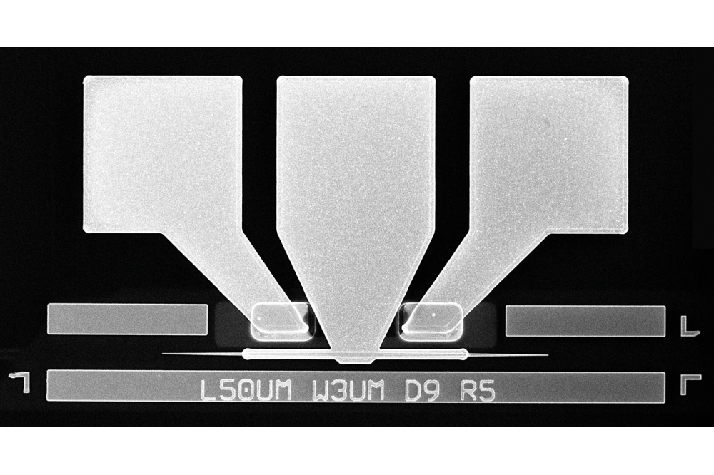
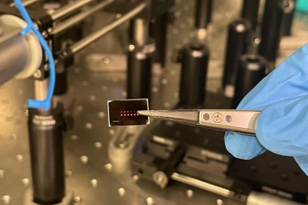
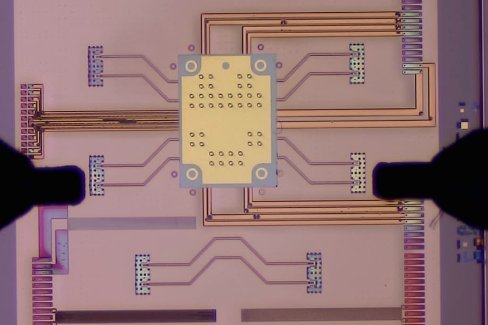
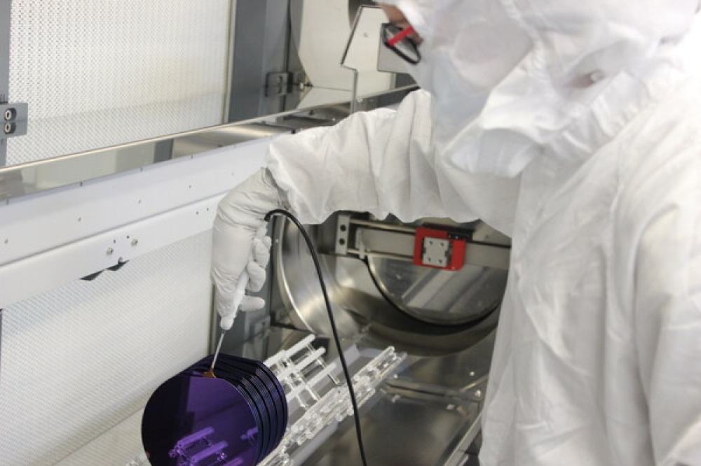
According to the company, the team has been working over the past three months to bring up the idled equipment, run epi wafer growth and regrowth from multiple MOCVD reactors, restart front-end micro-fabrication process through the line, and establish device testing, die preparation and separation processes in the back end. HieFo adds that the InP-based devices (lasers, gain chips, SOAs, PIN/APD detectors) produced from the resumed operations, have also passed reliability validation testing, thus ensuring that all original performance, quality and reliability standards will be met or exceeded.
Among the devices that are ready for volume production is a new chip design that HieFo says can support 1.6T single-carrier wavelength transceivers. According to the company, several leading optical module manufacturers have started placing orders with HieFo for its high-efficiency optical devices. HieFo says this accomplishment represents a significant milestone in its mission to deliver innovative solutions in the telecom, datacom, and AI connectivity industries.
“We are thrilled to announce the resumption of our optical devices production at the Alhambra facility,” said Genzao Zhang, CEO of HieFo Corporation. “This is a strong testament to HieFo’s dedication and commitment to maintaining continuity and excellence in the production of high-performance optical chips.”


