
Revolutionising optoelectronics with high-precision bonding

As data traffic looks set to outrun conventional pluggable optics, co-packaged optics is a promising innovation for powering our increasingly data-intensive world. However, this technology’s performance relies on extreme precision at the manufacturing stage. ASMPT AMICRA’s machines can meet this challenge.
BY MARCUS PLANCKH, HIGHTECH COMMUNICATIONS
Thanks to the rapid development of AI, the Internet of Things (IoT), 5G, and high-performance computing applications, datacentres have recently seen exponential growth in data traffic. Nearly three quarters of this remains within the confines of the datacentres. Meanwhile, with fibre-optic connections increasingly replacing copper cabling, the market for optical transceivers has been recording double-digit growth rates for several years. It is expected to reach a market volume equivalent to more than €14 billion by 2025. This is hardly surprising; fibre-optic technology has numerous advantages over traditional copper cabling, including saving on raw materials and energy, and offering high-bandwidth, low-loss signal transmission, even over long distances.
Wherever low-loss connections with very high data density are required, fibre optics are already being used today – for backbones in datacentres, for inter-datacentre connections, and for connections to 5G radio masts. Incidentally, besides traditional communications, optoelectronic technology can also be applied to biomedical sensors, augmented reality, power laser and automotive applications. For example, LiDAR, an optical method for measuring distance and speed using lasers, is one of the preferred technologies for 3D obstacle detection for autonomous driving. Many of these applications also require IoT connectivity, and thus additional computing power in datacentres.
In light of these dramatic developments, it is clear that fibre optics with conventional pluggable optics will not be able to keep pace with data communication requirements forever. But co-packaged optics (CPO) is offering a new way of powering today’s data-intensive world. The aim of this disruptive technology is to bring optical I/Os as close as possible to the ASIC switch, increasing bandwidth density and energy efficiency. Through advanced packaging and simultaneous optimisation of electronics and photonics, CPO – particularly on the silicon platform – can significantly reduce interconnect lengths, making it a promising technology for future datacentres.
This technology is being refined all the time, with the latest integration approach enabling CPO to use an external laser small form-factor pluggable (ELSFP) as the signal carrier. Laser light sources are placed externally at the faceplate of the SFP, and modulations kept at the CPO, while fibre connections replace the original copper traces. This approach maintains the function of CPO, while isolating heat sources from the core, increasing the feasibility of CPO development and deployment.

Figure 1. Example of a Chip-on-Carrier (COC) embedded in CPO: A laser COC is placed on a PIC wafer together with an electronic IC (EIC). This is then combined with an optical component and the application-specific IC (ASIC) on the substrate to form an optical engine (OE). (Image: ASMPT)
High-accuracy requirements
While CPO technology has enormous potential, it also faces challenges. In particular, it demands highly precise control of manufacturing and packaging processes, to ensure seamless connection between electronic and photonic components, as well as stability and reliability under extreme conditions. Standardising CPO technology remains an important industry task to address compatibility issues and drive market applications. For the latest CPO innovations and advanced solutions, ASMPT's precision equipment provides the photonics industry with the means to meet the higher integration demands of CPO.
To send bits through an optical fibre, electrical signals must first be converted into optical signals for transmission, and then converted back again at the end of the path. To do this, light-emitting and light-sensitive components must be connected to each other with such precision that scattering losses and attenuation are kept to an absolute minimum.
Discrete transceivers made up of many components are therefore comparatively large and difficult to produce. For example, each laser diode must be put into operation during assembly to make sure it is aligned correctly – a process also known as active alignment.
Modern semiconductor technologies can already replicate optical components, including waveguides and receivers, on substrates using CMOS lithography. The resulting PICs significantly reduce the number of separate components required for transceivers and therefore also the size and assembly costs. Laser diodes serve as light-emitting components in the optocouplers, which are placed and fixed directly onto the PICs using a die bonder.
The bonders are normally used in chip production to place semiconductor plates, known as dies, in a housing and to wire or solder them. They work so precisely that active alignment is no longer necessary when placing the laser diode, thus reducing assembly work and increasing fabrication productivity.

Figure 2. CPO with external laser SFP (ELSFP) as the signal carrier. Laser light sources are placed externally at the faceplate of the SFP, and modulations are kept at the CPO. Fibre connections replace the original copper traces. (Image: ASMPT)
The silicon photonics platform, which offers the greatest possible level of integration of electrical and optical components, requires a new generation of high-precision bonders. For example, a laser diode must be placed with an accuracy of <± 0.5 µm at 3 sigma (where sigma is a measure of process stability that relates extreme values and standard deviation). This is the only way to produce an optocoupler that meets the strict specifications for avoiding light scattering and reflection.
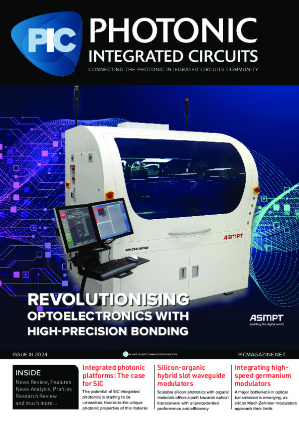
ASMPT, a market leader in this space, has developed such bonders with this high level of precision. With AMICRA, a proven platform is also available for optoelectronics. In fact, the AMICRA NANO model is the first in the industry to achieve a positioning accuracy of <± 0.2 µm at 3 sigma. Due to its unique precision, the AMICRA NANO is used wherever trend-setting, cutting-edge technology is required, including in research, for example. Its unrivalled accuracy is based on solid technology in multiple senses of the word; the entire positioning unit rests on a heavy, air-sprung granite plate to cushion it against external vibrations. The whole machine weighs around 2.5 tonnes.
Precision placement process
To begin with, the dies to be placed are fed individually or by pre-separated wafer. A very precise vacuum pipette then places them on a wafer or individual substrate. Another unique feature of the machine is that its so-called look-through placement head is designed in such a way that the high-resolution component camera can image the pipette from above. The camera works with a pixel size of 3.45 µm. There are three lenses that recognise line spacings between 1.66 and 5.56 µm.
Next, the pipette grips the die to be applied in such a way that it protrudes slightly on one side. This leaves fiducial marks visible on the die, which the system uses for orientation. There are corresponding fiducials on the substrate, which are also used for exact positioning.
As is usual in surface-mount technology (SMT), the part to be placed is first inspected, and will be rejected if it has visually recognisable defects. Once alignment is complete, the die is placed with a precisely defined bond force of between 0.2-0.20 N and then measured again. If the secondary measurement also shows values within the permissible tolerance range, the die is fixed by laser soldering, bonding, or a combination of contact pressure and heat.
The laser soldering step is enhanced by another special feature of the AMICRA NANO: the laser is aimed at the substrate from below through a glass plate. The advantage of this is that the elements are less sensitive to heat on their underside than they are on the top. A resistance heater integrated into the pipette also heats the component, which prevents positioning errors caused by thermal expansion and also improves the soldering behaviour. In total, this highly precise and complex
process requires a cycle time of 20-30 seconds. Some manufacturers therefore have 10 or more AMICRA NANOs working in parallel on one store floor. Overall, the process is far more efficient than discrete assembly.
For products with less stringent accuracy requirements, the AMICRA NOVA Pro bonder, also from the AMICRA platform, can offer shorter cycle times and more automation. This machine has a placement accuracy of <± 1 µm at 3 sigma, but significantly shorter cycle times (3-6 seconds at 1.5 µm, and 1.2-1.4 seconds at 5 µm). These machines also have great potential, due to the very wide range of CPO applications mentioned earlier.

Figure 3. AMICRA NANO: The bonder for processing optical and electronic components. The most precise machine currently on the market operates with a placement accuracy of <± 0.2 µm at 3 sigma. (Image: ASMPT)
Customised solutions
Today, no two electronics products have the same fabrication process. For this reason, the high-precision die bonders are generally designed individually and tailored to customer specifications. There is a wide range of options for customisation.
For example, software is available that can seamlessly trace all processed parts. This is particularly important to automotive suppliers, whose customers demand absolute traceability. AMICRA machines can also be equipped with a repair function that removes incorrectly positioned parts from the substrate, provided that this is technically possible. A flip-chip option is also part of the portfolio.
The growth of AMICRA's research and development department shows that high-precision bonding is now almost an industry in its own right. The Regensburg-based company was founded in 2001, has been part of ASMPT since 2018, and has enjoyed a steep growth curve right from the start. It currently has more than 130 employees. Last year, ASMPT opened its first European SEMI Center of Competence (CoC), at the AMICRA site in Regensburg, further supporting R&D by providing specialists and taking care of tests and evaluations.
With its market-leading machines, ASMPT is the only manufacturer to cover the entire process chain from wafer to assembled printed circuit board, and operates a large global network of R&D centres. These modern, pioneering laboratories have the latest machinery and equipment to demonstrate technologies and investigate the precise impact that innovations will have on electronics manufacturing, especially for CPO.
Dr. Johann Weinhändler, Managing Director at ASMPT AMICRA, sees the benefits of the CoC not least in the regional context: “We are delighted that we can now offer leading semiconductor companies and decision-makers in Europe the innovative ASMPT Semiconductor solutions and expertise at our centrally located CoC in Germany,” he says.
Dr. Weinhändler also points out that there are many reasons to be optimistic for the future: “The cloud market is growing infinitely. The demand for fast data rates and innovative applications is rising sharply, for example in datacentres. This goes as far as latency-free real-time transmissions. The situation is similar in future markets such as autonomous driving. Companies in this sector need ever smaller sensors and new technologies, just think of LiDAR.
However, this market also has enormous potential for us because it requires additional transmission stations almost everywhere, as every traffic light needs to be networked. These developments are fuelling our business with photonics and therefore systems for ultra-high-precision assembly.”

Dr. Johann Weinhändler, Managing Director at ASMPT AMICRA GmbH in Regensburg, is responsible for the Semiconductor Solutions Segment of ASMPT in EMEA. He is convinced that “the market for photonics and therefore for ultra-precise placement solutions will continue to grow enormously.” (Image: ASMPT)
The synthesis of optics and electronics marks a quantum leap, especially in communication technology, but also in many applications beyond it. High integration density in production is becoming increasingly important; the closer that components are brought together and the fewer individual parts need to be assembled per unit, the more effective, cheaper, and energy-efficient the product will be.
However, to achieve the next level of integration of the key technologies of silicon photonics and CPO, it is essential that production technologies also advance to new heights in precision and process stability. The AMICRA platform is already demonstrating the direction in which development must go. Machines such as the AMICRA NANO are setting standards that the industry must continue to follow in the future.


