
TOP-HIT consortium to use micro-transfer printing for heterogeneous integration

Tyndall National Institute, Cork, Ireland is leading a European consortium, called TOP-HIT, to develop novel technology that will address the challenge of integrating components of different materials in large volumes at the semi-conductor scale. The project is funded under the European Union's Horizon 2020 programme for Smart System Integration and is worth over €5M.
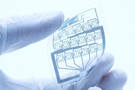
The TOP-HIT (Transfer-print operations for heterogeneous integration) consortium uses micro-transfer printing (µTP), a technology takes a set of devices out of one semiconductor wafer and prints these sparsely onto another wafer, transferring potentially many thousands of devices in each single transfer operation.
Brian Corbett, principal investigator at Tyndall and coordinator of the project explained: "The transfer print process, by combining diverse optical, electronic and other functional materials, opens up an enormous range of possibilities for new devices with embedded functionality.
"This will lead to more compact chips and systems for a variety of applications, such as telecommunications, smart sensing, biomedical sensing and data storage, but the key breakthrough will be the application of micro-transfer-printing to address the challenge of integrating non-compatible components in large volumes at the semiconductor wafer level, eliminating the need for current inelegant integration processes such as wire-bonding."
As an example of how this technique can be used, a small platelet of an expensive material could be picked up with a "˜stamp' (think of that platelet as being the ink attached to the stamp) and transferred (printed) with that same stamp onto a larger surface of another (cheaper) material. All the electrical and optical waveguide interconnections would be carried out on this second material. Alternatively, light emitting devices (such as LEDs or lasers) could be printed onto a material that is more suitable for electronic signal processing.
It is even possible to print several types of devices onto the same substrate material to combine, for example, light sources, detectors and signal processing. A "˜system-on-a-chip', a complex photonic integrated circuit (PIC) combining devices made of different materials, can be built up in this way. Printed platelets are typically a few microns thick, and can be printed with a placement precision of about 1 µm.
Tyndall's partners include X-Celeprint, Imec, Caliopa Huawei, Centre for Integrated Photonics, X-Fab, and Seagate.
X-Celeprint (Ireland) makes transfer printing equipment capable of printing many devices simultaneously. Research centre Imec (Belgium) has its own X-Celeprint equipment and provides the silicon photonics platforms that form the basis for the photonic products. Caliopa Huawei (Belgium) is a photonics company that develops optical components and circuits for telecommunications. The Centre for Integrated Photonics (CIP, a wholly owned subsidiary of Huawei, UK) develops InP based components and circuits for telecoms applications.
X-Fab (Germany), an analogue/mixed-signal and MEMS foundry, will develop new processes to provide wafers with components that can be transfer printed. It will add this capability to its existing portfolio of modular foundry processes. Seagate, a maker of hard disk drives and storage solutions. Tyndall (Ireland) co-ordinates the project, and provides designs and components that can be transfer printed by X-Celeprint onto platforms provided by Imec and X-Fab.


