
EV group organizes photonics workshop
EV Group (EVG), a supplier of wafer bonding and lithography equipment for the MEMS, nanotechnology and semiconductor markets, will host a special session at the 41st Micro and Nano Engineering (MNE 2015) conference--a leading international conference on micro- and nanofabrication and manufacturing using lithography and related techniques. The first EVG Photonics Workshop will take place at the World Forum in The Hague, The Netherlands, during the afternoon of the opening day of MNE 2015 on Wednesday, September 21.
Photonic applications are emerging rapidly, with photonic devices enabling new functionalities, smaller form factors, improved performance and reduced costs for broadband communications, sensing, bio-medical measurement devices and other applications. In particular, silicon photonics have received significant attention in recent years owing to their potential for enabling energy-efficient and affordable short-reach optical interconnects.
The EVG Photonics Workshop will bring together leading experts from device manufacturing and system suppliers to discuss flexible cooperation models, available platforms and applications, including nanoimprint lithography as an efficient manufacturing solution for photonic devices. The aim of this workshop is to foster the development of customer and industry partnerships, overcome the challenges and reduce the time to market for innovative photonic devices and applications. The EVG Photonics Workshop is free of charge. However, seating is limited and online registration is required at www.EVGroup.com/EVGPhotonicsWorkshop.
The EVG Photonics Workshop complements the company's other activities at MNE 2015. In addition to exhibiting at the show (booth #12), EVG is a collaborative partner on the Single Nanometer Manufacturing beyond CMOS devices (SNM) project, which will be the topic of an MNE special session, "Single Nanometer Manufacturing," on Tuesday, September 22 from 17:00 - 19:00.
The aim of the European Commission-funded SNM project is to establish new paths for manufacturing ultimate nanoscale electronic, optical and mechanical devices. 16 organizations from industry, academia and research institutes are participating in this unique project, which is headed by Professor Ivo W. Rangelow of the Technische Universität Ilmenau. The session will inform experts in lithography techniques and pattern transfer, metrology specialists and all other interested specialists about the latest and future developments in nanoscale manufacturing.
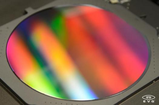
The goal of the first EVG Photonics Workshop at MNE 2015 is to foster the development of customer and industry partnerships, overcome the challenges and reduce the time to market for innovative photonic devices and applications. Topics of discussion will include flexible cooperation models, available platforms and applications, including nanoimprint lithography (NIL) as an efficient manufacturing solution for photonic devices. Shown here is a six-inch full-area nanoimprinted wafer processed by EVG NIL solutions. This technology enables almost infinite design freedom to create various kinds of photonic structures.
Full details on both events can be found on the MNE 2015 website at http://mne2015.org/programme/satellite-meetings/special-sessionsuser-meetings/


