Photonic ICs: reality check

Will US plans to drive integrated photonics forward finally deliver real products for real applications? Compound Semiconductor talks to industry executive, Michael Lebby, to find out more.
Late last year, President Obama revealed his intention to form his sixth Institute of Manufacturing Innovation; an Integrated Photonics Institute for Manufacturing Innovation.
Tasked with the key goal of developing cheap, high volume manufacturing methods for complex photonic integrated circuits in just five years, Universities across California, New York, Florida, Pennsylvania, have been rallying commercial support to establish industry-driven consortia.
With $110 million government funds at stake, not to mention mandatory matching in-kind contributions from industry, and potential contributions from local government, competition has been fierce.
Of the ten to twenty consortia that entered the first pre-proposal phase, only a maximum of four will be invited to submit a full proposal. These results are due at the end of this month, and a lone winner will follow.
"There is a shortlist process going on right now, but what is known is that three big consortia - from the Florida, New York and California areas - have emerged," explains Professor Michael Lebby from UK-based Glyndŵr University, and President of US-based start-up OneChip Photonics and optoelectronics consultancy, Oculi.
"New York is using its big silicon fab at Albany as an anchor, Florida has a strong optics community and California has MOSIS, a successful silicon foundry service," he adds.
Crucially, as Lebby highlights, the states of these 'big three' have promised to provide funds.
"We don't know how the Department of Defense will choose, but these three [consortia] have momentum," he says. "For example, California state has said it will match the federal money, so the proposal is already at $220 million, and New York and Florida states are expected to match contributions too."
Silicon leader
Lebby himself is a consultant for the Californian consortium, led by the Information Sciences Institute (ISI) at the University of Southern California USC, alongside the Universities of California Berkeley (UCB), Los Angeles (UCLA), San Diego (UCSD), Arizona State University, University of New Mexico and Ohio State University.
As hinted, this consortium is emulating its program on MOSIS, California's cost-cutting integrated circuit foundry service, formed back in 1981.
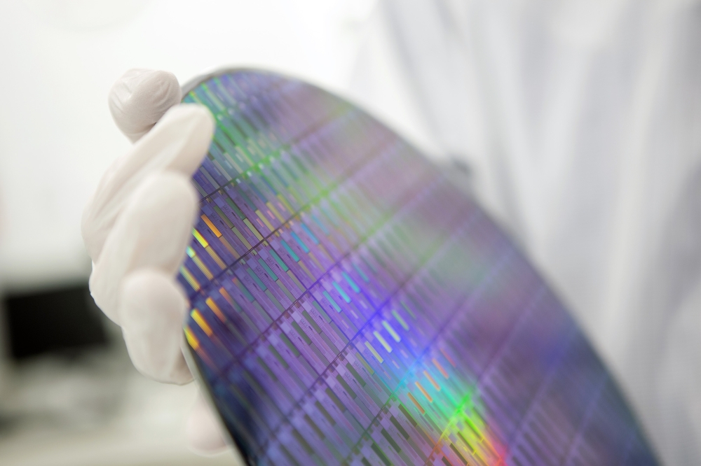
MOSIS - Metal Oxide Silicon Implementation Service - is operated by the USC's ISI and was set up to reduce chip costs by integrating numerous IC designs from different organisations onto a single wafer during fabrication. Designs are pooled into common lots and run through the fabrication process at foundries with the completed chips returned to customers.
Having prototyped more than 50,000 chip designs for private businesses, government agencies, research agencies and universities, this multi-project wafer approach has been very successful. And according to Lebby, this tactic will now be key to cutting integrated photonics technology costs.
"Whoever wins this competition is going to have to put a photonics MOSIS in place," he says."Integrated photonics technology is very expensive to develop, so people are trying to apply a the silicon industry's multi-wafer approach to the photonics industry."
As the industry executive highlights, MOSIS is a very successful silicon brokering system, with its multi-part wafer tactic being applied across the silicon industry.
"Having a III-V equivalent would be a very cool approach, and for California, this is certainly building on strengths, rather than starting from new," he adds.
But the notion of an integrated photonics foundry is hardly new. Thanks to more than a decade of European Commission funded programs, organisations across Europe have been busy trialling lines.
For example, Ghent University, Belgium, has been working with imec and CEA-LETI on a silicon photonics platform, while TU Berlin, Germany, and Lebniz-InstituteLeibniz-Institute IHP have established a silicon photonics opto-electronic IC pilot line.
And as Lebby points out: "As a continent, Asia also funds infrastructure a lot more aggressively than the US. From a competitive standpoint with Europe and Asia, the US is behind."
What's more, for these nations, following a shared foundry model has been key to the successes. The manufacture of complex integrated photonic circuits isn't cheap and sharing resources to cut costs has been imperative.
"To do a good job in silicon photonics, and even InP, you need fifty to one hundred million dollars, how many companies can afford that?" asks Lebby. "The [shared] foundry model means people can get integrated photonics at a lower cost structure. Europe already figured this out, Japan has figured this out and America has just figured this out."
![]()
President Obama has finally announced his administration's intent to create an integrated photonics institute for manufacturing innovation [White House]
For its part, the latest US program now intends to develop an 'onshore' integrated photonics manufacturing line, in a bid to stem the steady stream of home-grown photonics technology to Asia-based nations.
The initial platform will focus on photonic interconnects for data centres and the winning consortium will home in on four key areas; RF photonics, optoelectronics sensing, digital communications, and packaging and assembly.
Crucially for the future of integrated photonics, other funding programs, such as the EU's Horizon 2020, are already calling for integrated photonics lines to produce qualified products. And the US is following suit.
"Integrated photonics is now at a point where the [product] coming out of the foundry, pilot line needs to be used in real products by customers," he says. "US government wants industry to use these consortia to run pilot line to get prototypes, this is important as the stuff coming out of any pilot line must be accepted by industry as a qualified product."
"Many want to see silicon photonics for real and a lot of money is being invested. There's a lot of hope out there," he adds.


