Loading...
News Article

US DoD launches competition for Integrated Photonics Manufacturing Institute

$100 million in federal investment matched by $100 million or more in private investment to the winning consortia 

The US Department of Defense is launching a competition to award more than $100 million in federal investment matched by $100 million or more in private investment to the winning consortia to build a new Institute for Manufacturing Innovation (IMI) focused on Integrated Photonics, President Obama announced today.

This Institute will focus on developing an end-to-end photonics "˜ecosystem' in the US, including domestic foundry access, integrated design tools, automated packaging, assembly and test, and workforce development.

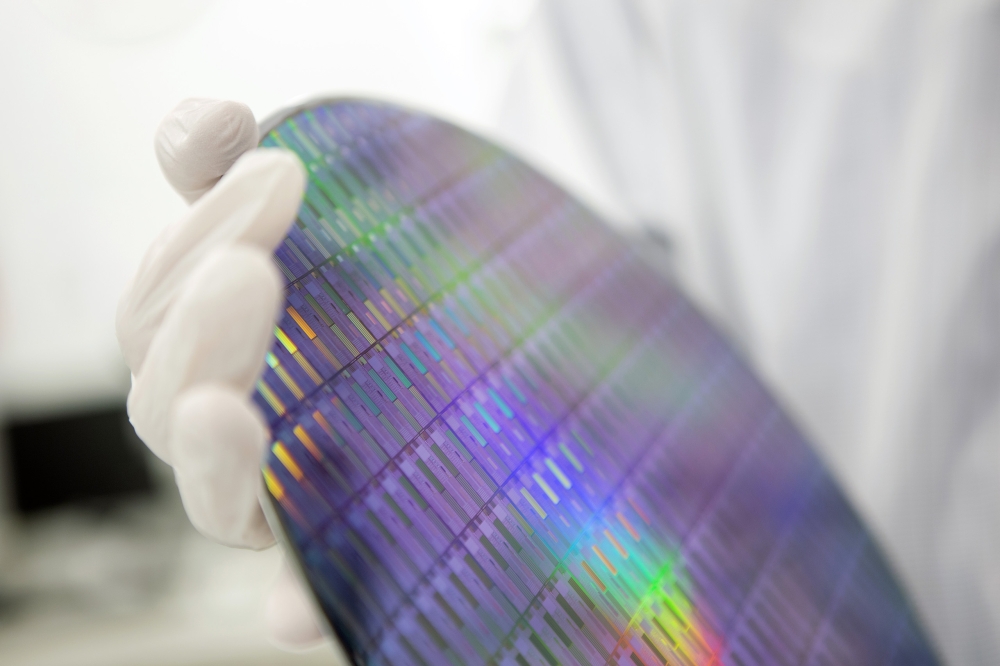
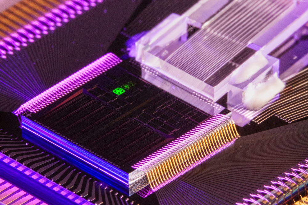
Photonics, the use of light for applications as diverse as lasers and telecommunications, powers the Internet as we know it today. Integrated photonics manufacturing, the next generation of this of technology, involves integrating electronic and photonics technologies into single systems rather than the assortments of discrete units that exist now. Realising these opportunities requires development of high-volume mass-manufacturing, assembly, and packaging technologies and processes that are reliable and cost-effective. 

Compound III-V semiconductors such as GaA, InP, and InGaAs are considered key technologies within photonics. They are used for making light emitting structures including solid state lasers and LEDs and components such as optical amplifiers

Beyond the Internet and telecommunications, integrated photonics is expected to be important in medicine "“ from the development of 'needleless' technologies for monitoring diabetics' blood sugar levels to tiny cameras smaller than pills that can travel within arteries. It is also hoped that integrated photonic technology will make human genomes sequencing cheaper bringing it well below $1,000 as compared to $5,000 today.  In defence applications potential uses of integrated photonics range from improving battlefield imaging to advances in radar. 

The Integrated Photonics Manufacturing Institute  - with over $200 million in public and private resources - is expected to comprise the largest Federal investment to date, reflecting the complexity of this technology, its importance to national security, and its revolutionary potential. 

Lightwave Logic receives ECOC Innovation Award for Hybrid PIC/Optical Integration Platform
Coherent wins ECOC award for datacentre innovation
HyperLight announces $37 million funding round
Jabil expands silicon photonics capabilities
Ephos raises $8.5 million for glass-based photonic chips
Designing for manufacture: PAM-4 transmitters using segmented-electrode Mach-Zehnder modulators
OpenLight and Epiphany partner on PIC ecosystem
NewPhotonics and SoftBank team up on advanced photonics
POET and Mitsubishi collaborate on 3.2T optical engines
Integrated photonic platforms: The case for SiC
Integrating high-speed germanium modulators with silicon photonics and fast electronics
Lightium Secures $7 Million Seed Funding
Revolutionising optoelectronics with high-precision bonding
Fraunhofer IMS invites participation in PIC engineering runs
Advances in active alignment engines for efficient photonics device test and assembly
Aeva announces participation at IAA Transportation 2024
Sumitomo Electric announces participation in ECOC 2024
Quside receives NIST certification for quantum entropy source
DustPhotonics launches industry-first merchant 1.6T silicon photonics engine
Arelion and Ciena announce live 1.6T wave data transmission
DGIST leads joint original semiconductor research with the EU
POET Technologies reorganises engineering team
A silicon chip for 6G communications
South Dakota Mines wins $5 million from NSF for Quantum Materials Institute
HieFo indium phosphide fab resumes production
Coherent launches new lasers for silicon photonics transceivers
AlixLabs wins funding from PhotonHub Europe
Sandia National Labs and Arizona State University join forces
Perovskite waveguides for nonlinear photonics
A graphene-based infrared emitter
Atom interferometry performed with silicon photonics
A step towards combining the conventional and quantum internet

×
Search the news archive

To close this popup you can press escape or click the close icon.
Logo
x
Logo
×
Register - Step 1

You may choose to subscribe to the PIC Magazine, the PIC Newsletter, or both. You may also request additional information if required, before submitting your application.


Please subscribe me to:


You chose the industry type of "Other"

Please enter the industry that you work in: