Technical Insight
Uniting silicon and InP to make versatile, low-cost photonic chips
Telecom and datacom networks are under ever-increasing strain from an explosion in data transfer. What's the long-term solution? It's a universal photonics technology that marries InP performance with large silicon wafers, argue Daniel Sparacin and Greg Fish from Aurrion.
It takes just a yearand a half for the bandwidth demand for telecommunications networks to double. The primary drivers for this are the soaring number of networked devices – half of Americans now have smart phones – and an increase in data downloaded from the likes of Netflix, Amazon and iTunes.
Rocketing levels of data transfer don’t just strain the telecom networks – they also create an unprecedented challenge for their datacom siblings. Lying at the heart of these datacom networks are datacenters, which are used for a diverse range of applications and can often feature tens of thousands of servers. These servers require flexible, agile interconnect networks, which must be capable of allocating jobs to any server, at any time, to respond to user demand.
The telecom and datacom networks, which work together to control the flow of internet traffic, place different demands on the evolution of the underlying interconnect technology. Long-haul telecom technology is optimised for spectral efficiency and high bandwidth, due to the cost of deploying fibers in the field. In comparison, short-reach datacom technology offers a cost-effective, low-power approach for connecting extremely large numbers of data ports in a single location. These differences account for the need for: high-performance components in telecom networks; and for lower-cost components, which can be made in far higher volumes, in datacom networks.
Scaling issues
Products for serving both of these networks must deliver increases in performance as their dimensions are reduced. This performance-scaling requirement suggests that the only viable route ahead is a chip-based approach, rather than conventional discrete component assembly. This should cater for increases in the bandwidth requirements per transceiver, along with its complexity and component count.
It is tough to scale existing photonic technologies for datacom networks, because next-generation products have to be cheaper, produced in higher volumes, run off less power, and be housed in smaller packages. On the long-haul side of the industry, the focus has been on developing high-performance transceivers based on complex, InP-based photonic integrated circuits (PICs). These chips have satisfied performance requirements, but if they are to meet the cost and volume needs of datacentre interconnects, a significant ramp in manufacturing capability must occur. Today, the incumbent technology in that sector is a combination of VCSELs and multi-mode fiber. This product serves low-cost, high-volume markets by delivering high aggregate bandwidths, but it lacks sufficient reach for large datacentres.
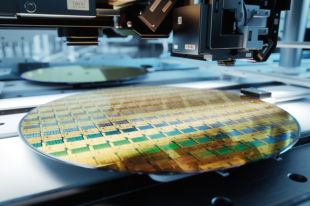
In contrast, silicon photonics – a relatively new area of the photonics industry – promises to provide a platform that will scale to fulfill the demands of next-generation datacom interconnects. Its attractive features include: the ability to digitally enhance photonics through co-design of optical devices in silicon with electronics; the leveraging of high-precision, shared foundries using wafers with diameters of up to 12-inches; and silicon’s compatibility with the developments in advanced packaging. The latter attribute means that there is potential to move photonics out of a ‘gold box’ package and into one with intimate interconnection to the electronic chip.
Despite all its potential, commercial realization of silicon photonics is taking longer than many had hoped for. Up until now, the laser has been segregated from the rest of the chip, leading to compromised system architecture: The laser is then treated like a power supply and split into many parallel channels, leading to a hike in cabling costs, rather than utilising the spectrally allocated bandwidth provided by wavelength division multiplexing (WDM) systems.
One upshot of separating the laser from the rest of the chip is that it delays penetration of silicon photonics into datacom markets. Performance is also compromised, preventing this technology from impacting most telecom markets. However, early work in heterogeneous integration by groups at Intel, Ghent University and the University of California, Santa Barbara, has shown that it is possible to overcome these issues by turning to a radically different architecture – one that uses silicon to define a laser’s cavity, while using III-V materials to provide efficient gain.
Commercialising hetero-integration
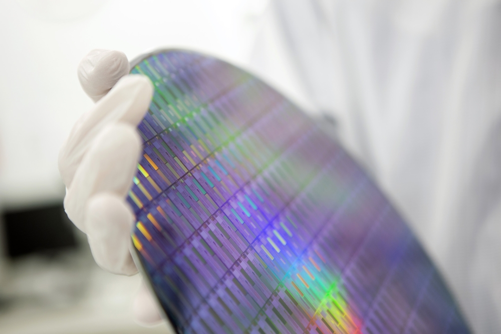
At Aurrion of Goleta, CA, we have developed a heterogeneous platform for integrating InP-based semiconductor materials onto existing silicon photonic substrates. This enables all photonic functions, including the laser, to be brought together onto a single chip. The basic underlying photonic circuit, comprised of low-loss silicon and dielectric waveguides, is generated on a silicon-on-insulator substrate using established foundry infrastructure. Thanks to this approach, cost advantages result from: the leveraging of shared resources; the use of 8-inch substrates, rather than 2-inch substrates, the common platform for photonics; and superior yield, which stems from higher-capacity foundries with greater capability and better quality systems, compared with traditional III-V photonics fabrication facilities.
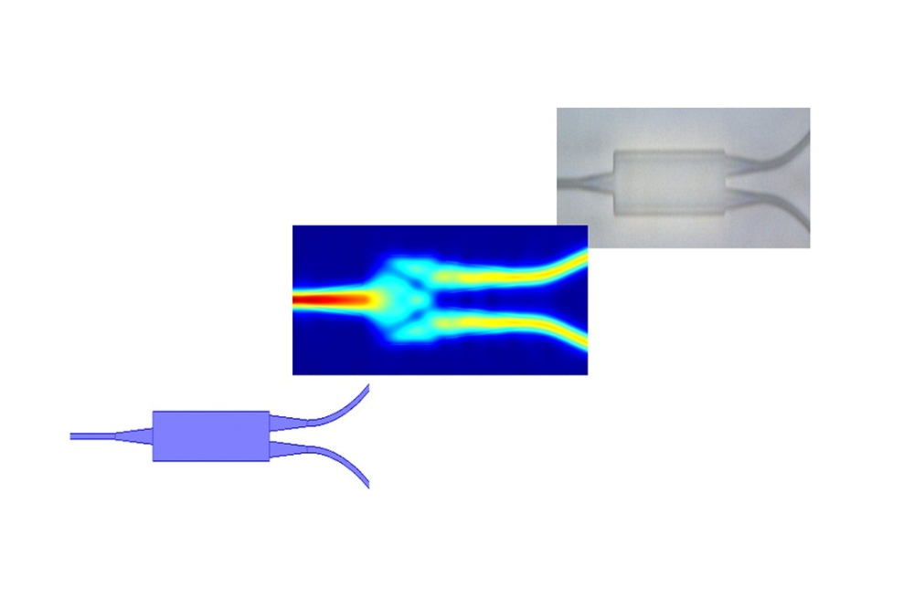
Our process features a bonding step to add InP functionality to the photonic circuits at the wafer-scale. This involves placing ‘chiplets’ of custom unprocessed InP epitaxial material on the silicon photonic circuit. Using standard semiconductor lithography and etch steps, InP-based chiplets are processed in parallel to form lasers, optical amplifiers, modulators and photodetector devices. In every case, they are registered to the underlying waveguides and optically connected through evanescent mode converters, which provide a conduit between the silicon and InP layers for the optical mode propagating through the circuit.
Once that has been carried out, further processing steps encapsulate InP with dielectric materials, and also form metal interconnects and contacts for driver and control circuitry. Finally, the chip is housed in a package, using technologies developed for the electronics industry. By being able to take advantage of the developments in that mature sector, we are able to use 2.5D or 3D interposer technologies to tightly integrate our photonic chip with advanced node electronic driver chips.
One of the attractive features of heterogeneous integration is that it allows a wide choice of gain materials, which do not have to be placed on the silicon chip with a tremendous degree of accuracy. Thanks to this, it is possible to process photonic circuits operating in disparate wavelength regimes side-by-side on the same chip. We have recently demonstrated this capability to deliver photonic laser sources for telecom and datacom applications united on a single wafer (more details can be found in B. R. Koch et. al.“Integrated Silicon Photonic Laser Sources for Telecom and Datacom,” in Optical Fiber Communication Conference/National Fiber Optic Engineers Conference 2013, OSA Technical Digest (Optical Society of America, 2013), paper PDP5C.8).
What’s more, our capability to integrate multiple, tailored InP quantum well epitaxial materials throughout the photonic circuit provides us with a silicon integration platform that permits the unique realisation of high performance InP-based active devices and silicon-based passive devices on a single chip. This means that in addition to an InP-based laser, we can build circuits featuring InP-based modulator and detector devices, which deliver superior electro-optic performance compared with traditional silicon photonic p-i-nmodulators and germanium detectors.
Arguably, by far the biggest benefit of our heterogeneous integration platform is that it enables a manufacturing capability that can process a variety of PICs simultaneously. This can usher in a new era, assigning the one-product/one-process cost-structure to the history books. Lower-volume photonic components operating at unique wavelengths, such as telecom or military focused PICs, can then be produced on the same lines used to make higher-volume components, such as datacom interconnects or fiber-access network transceivers. This will break the strong tie between volume and cost, leading to new application areas and wider usage of photonic components.

Figure 3. Aurrion’s unique heterogeneous integration process enables coherent 100G telecom transmitters and 16 channel 400 Gbit/s datacom transmitters to be fabricated simultaneously on the same silicon wafer using existing foundry infrastructure
Promising prototypes
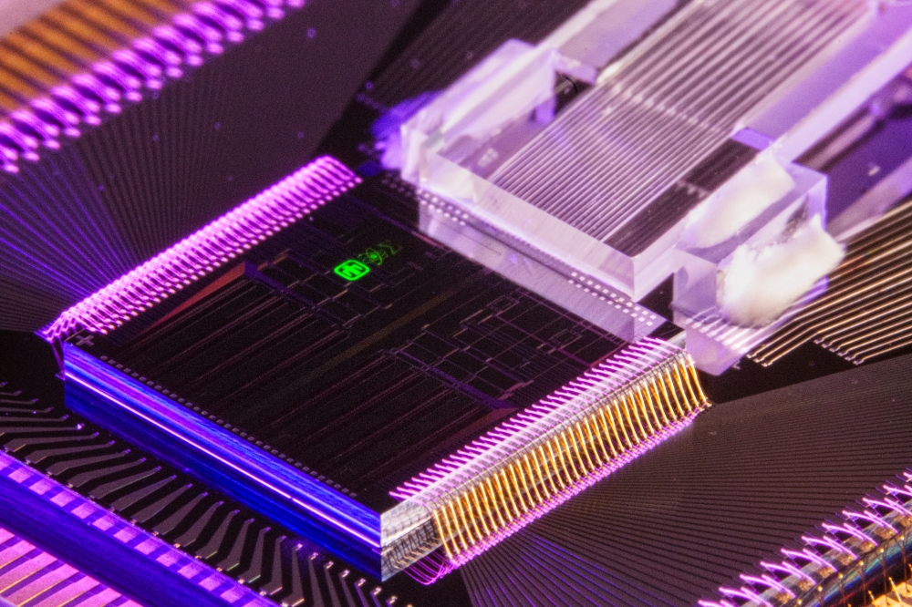
Our photonic technology is directly applicable to several near-term datacom and telecom transmitter needs, including an uncooled 16-channel fixed wavelength datacom laser array that we have produced (see Figure 4). This array not only provides a path for a less expensive version of current 100G standards, such as the IEEE 100GBASE-LR4, which only requires 4 laser wavelengths – it also addresses the recently announced 400 Gbit/s Ethernet standard that could be defined for 16 laser wavelengths. By further integrating this existing laser array with modulators, photodetectors, wavelength multiplexors and demultiplexors – library components which already exist in the silicon photonic toolbox – it is possible to realize a chip-scale, multi-channel WDM silicon photonic transmitter that can finally address existing and future standards.

Figure 4. 16-channel fixed-wavelength laser array fabricated on silicon and suitable for datacom transmitters
Similarly, our telecom wavelength laser, which produces in excess of 20 mW and can be tuned over more than 45 nm, can be readily integrated on a single chip with coherent modulators and polarization diversity optics to meet OIF 100G standards for metro telecom applications.
In both the examples just described, the unique attributes of our heterogeneous integration platform enable a complex, highly functional single-chip product that can be manufactured at a relatively low cost. Such a chip can scale with the requirements of current and future generations of datacom and telecom interconnect technologies, providing the bandwidth, density and cost needed over the coming decades.
Rocketing levels of data transfer don’t just strain the telecom networks – they also create an unprecedented challenge for their datacom siblings. Lying at the heart of these datacom networks are datacenters, which are used for a diverse range of applications and can often feature tens of thousands of servers. These servers require flexible, agile interconnect networks, which must be capable of allocating jobs to any server, at any time, to respond to user demand.
The telecom and datacom networks, which work together to control the flow of internet traffic, place different demands on the evolution of the underlying interconnect technology. Long-haul telecom technology is optimised for spectral efficiency and high bandwidth, due to the cost of deploying fibers in the field. In comparison, short-reach datacom technology offers a cost-effective, low-power approach for connecting extremely large numbers of data ports in a single location. These differences account for the need for: high-performance components in telecom networks; and for lower-cost components, which can be made in far higher volumes, in datacom networks.
Scaling issues
Products for serving both of these networks must deliver increases in performance as their dimensions are reduced. This performance-scaling requirement suggests that the only viable route ahead is a chip-based approach, rather than conventional discrete component assembly. This should cater for increases in the bandwidth requirements per transceiver, along with its complexity and component count.
It is tough to scale existing photonic technologies for datacom networks, because next-generation products have to be cheaper, produced in higher volumes, run off less power, and be housed in smaller packages. On the long-haul side of the industry, the focus has been on developing high-performance transceivers based on complex, InP-based photonic integrated circuits (PICs). These chips have satisfied performance requirements, but if they are to meet the cost and volume needs of datacentre interconnects, a significant ramp in manufacturing capability must occur. Today, the incumbent technology in that sector is a combination of VCSELs and multi-mode fiber. This product serves low-cost, high-volume markets by delivering high aggregate bandwidths, but it lacks sufficient reach for large datacentres.
In contrast, silicon photonics – a relatively new area of the photonics industry – promises to provide a platform that will scale to fulfill the demands of next-generation datacom interconnects. Its attractive features include: the ability to digitally enhance photonics through co-design of optical devices in silicon with electronics; the leveraging of high-precision, shared foundries using wafers with diameters of up to 12-inches; and silicon’s compatibility with the developments in advanced packaging. The latter attribute means that there is potential to move photonics out of a ‘gold box’ package and into one with intimate interconnection to the electronic chip.
Despite all its potential, commercial realization of silicon photonics is taking longer than many had hoped for. Up until now, the laser has been segregated from the rest of the chip, leading to compromised system architecture: The laser is then treated like a power supply and split into many parallel channels, leading to a hike in cabling costs, rather than utilising the spectrally allocated bandwidth provided by wavelength division multiplexing (WDM) systems.
One upshot of separating the laser from the rest of the chip is that it delays penetration of silicon photonics into datacom markets. Performance is also compromised, preventing this technology from impacting most telecom markets. However, early work in heterogeneous integration by groups at Intel, Ghent University and the University of California, Santa Barbara, has shown that it is possible to overcome these issues by turning to a radically different architecture – one that uses silicon to define a laser’s cavity, while using III-V materials to provide efficient gain.
Commercialising hetero-integration
At Aurrion of Goleta, CA, we have developed a heterogeneous platform for integrating InP-based semiconductor materials onto existing silicon photonic substrates. This enables all photonic functions, including the laser, to be brought together onto a single chip. The basic underlying photonic circuit, comprised of low-loss silicon and dielectric waveguides, is generated on a silicon-on-insulator substrate using established foundry infrastructure. Thanks to this approach, cost advantages result from: the leveraging of shared resources; the use of 8-inch substrates, rather than 2-inch substrates, the common platform for photonics; and superior yield, which stems from higher-capacity foundries with greater capability and better quality systems, compared with traditional III-V photonics fabrication facilities.
Our process features a bonding step to add InP functionality to the photonic circuits at the wafer-scale. This involves placing ‘chiplets’ of custom unprocessed InP epitaxial material on the silicon photonic circuit. Using standard semiconductor lithography and etch steps, InP-based chiplets are processed in parallel to form lasers, optical amplifiers, modulators and photodetector devices. In every case, they are registered to the underlying waveguides and optically connected through evanescent mode converters, which provide a conduit between the silicon and InP layers for the optical mode propagating through the circuit.
Once that has been carried out, further processing steps encapsulate InP with dielectric materials, and also form metal interconnects and contacts for driver and control circuitry. Finally, the chip is housed in a package, using technologies developed for the electronics industry. By being able to take advantage of the developments in that mature sector, we are able to use 2.5D or 3D interposer technologies to tightly integrate our photonic chip with advanced node electronic driver chips.
One of the attractive features of heterogeneous integration is that it allows a wide choice of gain materials, which do not have to be placed on the silicon chip with a tremendous degree of accuracy. Thanks to this, it is possible to process photonic circuits operating in disparate wavelength regimes side-by-side on the same chip. We have recently demonstrated this capability to deliver photonic laser sources for telecom and datacom applications united on a single wafer (more details can be found in B. R. Koch et. al.“Integrated Silicon Photonic Laser Sources for Telecom and Datacom,” in Optical Fiber Communication Conference/National Fiber Optic Engineers Conference 2013, OSA Technical Digest (Optical Society of America, 2013), paper PDP5C.8).
What’s more, our capability to integrate multiple, tailored InP quantum well epitaxial materials throughout the photonic circuit provides us with a silicon integration platform that permits the unique realisation of high performance InP-based active devices and silicon-based passive devices on a single chip. This means that in addition to an InP-based laser, we can build circuits featuring InP-based modulator and detector devices, which deliver superior electro-optic performance compared with traditional silicon photonic p-i-nmodulators and germanium detectors.
Arguably, by far the biggest benefit of our heterogeneous integration platform is that it enables a manufacturing capability that can process a variety of PICs simultaneously. This can usher in a new era, assigning the one-product/one-process cost-structure to the history books. Lower-volume photonic components operating at unique wavelengths, such as telecom or military focused PICs, can then be produced on the same lines used to make higher-volume components, such as datacom interconnects or fiber-access network transceivers. This will break the strong tie between volume and cost, leading to new application areas and wider usage of photonic components.
Figure 3. Aurrion’s unique heterogeneous integration process enables coherent 100G telecom transmitters and 16 channel 400 Gbit/s datacom transmitters to be fabricated simultaneously on the same silicon wafer using existing foundry infrastructure
Promising prototypes
Our photonic technology is directly applicable to several near-term datacom and telecom transmitter needs, including an uncooled 16-channel fixed wavelength datacom laser array that we have produced (see Figure 4). This array not only provides a path for a less expensive version of current 100G standards, such as the IEEE 100GBASE-LR4, which only requires 4 laser wavelengths – it also addresses the recently announced 400 Gbit/s Ethernet standard that could be defined for 16 laser wavelengths. By further integrating this existing laser array with modulators, photodetectors, wavelength multiplexors and demultiplexors – library components which already exist in the silicon photonic toolbox – it is possible to realize a chip-scale, multi-channel WDM silicon photonic transmitter that can finally address existing and future standards.
Figure 4. 16-channel fixed-wavelength laser array fabricated on silicon and suitable for datacom transmitters
Similarly, our telecom wavelength laser, which produces in excess of 20 mW and can be tuned over more than 45 nm, can be readily integrated on a single chip with coherent modulators and polarization diversity optics to meet OIF 100G standards for metro telecom applications.
In both the examples just described, the unique attributes of our heterogeneous integration platform enable a complex, highly functional single-chip product that can be manufactured at a relatively low cost. Such a chip can scale with the requirements of current and future generations of datacom and telecom interconnect technologies, providing the bandwidth, density and cost needed over the coming decades.


