Technical Insight
Increasing the versatility of photonic integrated circuits
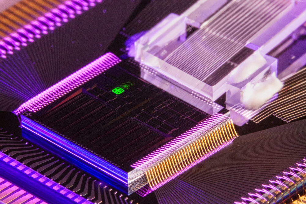
Photonic integrated circuits enable the construction of compact, highly functional components, but operation tends to be restricted to telecom wavelengths. We are now addressing this shortcoming by developing devices that operate further into the infrared, say imec's Dries Van Thourhout and Gunther Roelkens.
If you want to combine several functions on a single chip, you can build an integrated circuit (IC). In its electronic form this device is now incredibly mature, but the same cannot be said for its photonic counterpart. That’s partly because more than 95 percent of electronic IC’s are made in silicon, while a vast and varied array of materials are employed for fabricating optical PIC’s, including III-Vs, polymers, glass and LiNbO3. This diversity in materials has diminished the advantages that come with scaling, and accounts for this class of ICs’ relatively low degree of integration and suboptimal performance.
These weaknesses have been known for many years, and since the 1990s several research groups have tried to address this by turning to silicon as a substrate for making these optical circuits. Its attributes include optically transparency in the telecommunication window (1300 nm and 1550 nm), plus a very high index contrast with the surrounding air or glass, which enables extremely compact circuits. What’s more, optical PIC’s can be fabricated with the same set of tools as those used to manufacture their electronic cousins. This means that PIC production can take advantage of the installed manufacturing base, spurring the development of new types of circuit that combine a higher degree of integration with lower costs, higher performance and even co-integration with electronics.
During the last decade this new waveguide platform has been integrated with high performance passive circuitry and filters, low loss optical switches, high-speed optical modulators and germanium-based photodetectors. However, due to its indirect bandgap, it is incredibly difficult to obtain direct light generation from silicon. The most promising structures for generating light emission are silicon nanocrystals and strained germanium, and both of these are the subject of intense investigation. However, these devices are vastly inferior to conventional devices built from III-Vs.
To address this situation, our team at imec – and also other research groups, such as those based at CEA-LETI, France, and the University of California, Santa Barbara (UCSB) – have developed technologies for taking high-quality III-V epitaxial layers grown on a native substrate and transferring them to silicon wafers. With this approach we have formed circuits operating at telecom wavelengths that unite single-wavelength lasers and detector arrays, both containing InP-based active layers, with high-precision silicon nanophotonics wavelength demultiplexers. In addition, more recently we have highlighted the true versatility of this approach by also integrating GaSb-related materials on silicon: This has led to the first ever demonstration of waveguide-based spectrometers operating above 2 mm.
Wafer bonding
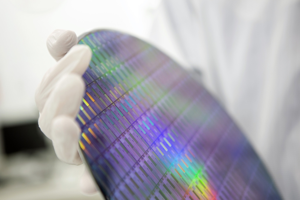
The heart of our integration process is the bonding of III-V die or wafers to silicon with an adhesive layer – the thermosetting polymer DVS-BCB, which is available from Dow Chemical (see Figure 1). We have spent several years optimizing this bonding process, and it is now possible to reliably bond with intermediate adhesive layers less than 50 nm-thick, while realizing within wafer and wafer-to-wafer accuracy below 3 nm. With our technology we can perform wafer-to-wafer bonding, die-to-wafer bonding, and even simultaneous bonding of dies with different thickness.

Figure 1. Illustration of the bonding process. The starting point is the processed SOI-wafer (a) with silicon waveguides. For building more advanced PICs this wafer may also already contain active devices such as modulators and germanium detectors. Next, dies or wafers of unprocessed III-V material are bonded on top, with the epitaxial layers oriented towards the silicon waveguides (b). Then the substrate is removed using grinding and or wet/chemical etching, such that only a thin stack with the active layers remains on the silicon wafer (c). This wafer can now be further processed using standard wafer-scale processing techniques such as deep UV lithography, mesa etching (d) and metallization (e), resulting in finished chip as shown in (f).
We are not the only group to have developed a bonding technology. Researchers at UCSB use direct bonding after oxygen plasma activation to attach one material to another, while engineers at CEA-LETI employ a technique that they describe as molecular bonding, which is based on the mating of two oxide-clad wafers. Both these approaches have the advantage of avoiding a polymer layer in the stack, but they are more sensitive to surface roughness and contamination. Note that in all cases the overall integration philosophy remains the same.
Once the materials have adhered to one another, the substrate of the bonded material is removed to leave a high quality III-V epitaxial layer on the silicon platform. This thickness of this III-V structure can range from less than 100 nm to 2 μm – its value should reflect the target application. From that point onwards, fabrication can exploit standard waferscale processes. This means that the accuracy of alignment between III-V devices and silicon waveguides is determined by lithographic processes. These deliver far tighter tolerances than the flip-chip process used for integrating prefabricated devices on top of a wafer.

Figure 2 a) Bonded wafer, in this case on a transparent Pyrex wafer, allowing us to inspect the interface, showing no defects in this case b) Multiple bonded InP dies on a patterned SOI substrate c) Cross-section of bonded InP wafer on silicon waveguide
Making lasers ……
Our device development began with the fabrication of telecom-wavelength lasers based on InP and related material. We constructed a portfolio of emitters, ranging from simple Fabry-Perot lasers to single-longitudinal-mode, DFB-type lasers – with the grating defined in the silicon layer – and more complex devices, such as tuneable lasers. The latter, which featured advanced filters in the silicon layer to provide wavelength-selective feedback, has typical threshold currents of 25-50 mA and delivers output powers up to 10 mW.
One of the biggest challenges associated with the fabrication of PICs incorporating lasers is realising efficient coupling of light out of this device and into silicon. This can be achieved with the ‘hybrid laser’, a design originally proposed by UCSB, which maintains the optical mode within the silicon waveguide – its evanescent tail extends into the III-V gain layers on top. We have adopted this approach to build a DFB laser using our BCB-bonding process (see Figure 3). This device contains eight InGaAlAs based quantum wells, optimized for emission at 1.3 μm.

Figure 3. Ultra-dense wavelength demultiplexer chip developed in the EU-funded project BOOM. a) Top view of chip. b) Eye diagram for detector under 10GBit/s operation. c) Full optical to electrical response of the device.
Another, more common approach for us is to concentrate light into the III-V layers and couple it back to the silicon layer using evanescent tapers. By creating suitable structures in the silicon layer, it is possible to have wavelength selective feedback, leading to single-mode operation. We have helped to build this type of structure in an EU project called HELIOS, working in partnership with CEA-Leti and III-V lab, France, who provided silicon waveguide circuits and III-V processing, respectively (see Figure 3).
A ring resonator and a grating-based mirror in the silicon layer form the laser cavity, and the III-V layer provides the needed gain. The device delivers up to 10 mW, has threshold currents below 40 mA, and features a side-mode suppression in excess of 30dB. Tuning the ring resonator – in this case via the thermo-optic effect – enables wavelength tuning over 5 nm to 10 nm.
…. and detectors
We can also integrate InGaAs-based detectors with our silicon photonic circuits. Our involvement in the EU-project BOOM has required this, because this programme requires an optical label detector. One of the goals of this project is to label optical data packets with an inband wavelength code, which has to be extracted from the packet and sent to a routing unit. This allows full optical routing of IP-packets, without decreasing the spectral efficiency of the system.]. The label extractor consists of an optical demultiplexer with very high resolution – 12.5 GHz – fabricated on our silicon photonics platform and integrated with high efficiency photodetectors.
It has been very challenging to reach the required resolution, with success only possible after an in-depth study of silicon micro-ring resonators. This analysis revealed that the required specifications could be reached with single ring-resonator-based filters. These resonators have integrated resistors, which allow fine-tuning of the wavelength channels (bottom electrodes) through the thermo-optic effect. They are connected to evanescently coupled InGaAs photodetectors using heterogeneous integration technology developed by INTEC, imec’s associated laboratory at Ghent University.
The efficiency of these detectors is almost 1A/W, and they can operate at a speed of 5GBit/s considerably higher than the 1GBit/s specification set forward at the start of the project. Engineers at Fraunhofer IZM group in Berlin have helped to package this device, which is now ready for operation in a system test bed.

Figure 4 a) Hybrid DFB-laser. b) Schematic of III-V silicon tunable laser. c) Spectral response of III-V silicon tunable laser, for different values of tuning power on integrated ring resonator.
Heading further into the infrared
Our efforts at developing PICs started with the development of devices operating at telecom wavelengths. We are now expanding the spectral range of the devices that can be made, because this allows circuits to serve different applications. For example, devices operating in the short-wave (SWIR) and mid-wave (MWIR) infrared wavelength ranges, which span 2 μm to 8μm, could be used for spectroscopic sensing. That’s because there are numerous gas, liquid and solid absorption features in this spectral domain.
To date, there have been very few, if any, complex PICs that have been built to work in this spectral range. Progress has been hampered by difficulties associated with developing an integration process that is fully monolithic – in other words, one that is based completely on III-V semiconductors. We try to address the lack of progress in this area by employing our heterogeneous integration process to develop such circuits.
One of the strengths of silicon photonics is its broad transparency window, which stretches from 1 μm to 4 μm. Thanks to this, it should be possible to realize integrated spectroscopic systems combining active III-V devices and silicon-on-insulator passive circuits. Such systems could be incredibly compact, highly affordable and superior to existing products in terms of selectivity and sensitivity.
Fabrication of these systems requires integration of short-wave and mid-wave infrared light sources and photodetectors on top of the silicon waveguide circuit. Our first step towards this was to demonstrate efficient detectors integrated with a silicon-based integrated spectrometer circuit. The detector built for this, which was bonded to a silicon waveguide circuit, had an epilayer stack featuring a 500 nm-thick Ga0.79In0.21As0.19Sb0.81 layer as the intrinsic absorbing region (see Figure 5). Antimonide layers were grown by the Institut d’Electronique du Sud from the university of Montpellier.

Figure 5 a) Cross-section of evanescently coupled InGaAsSb-detector integrated on silicon waveguide. b) Current-voltage and current-power characteristics for this detector under illumination at 2.25 μm.
Evanescently coupled detectors fabricated in this way produce a responsivity of 1.4 A/W at 2.3 μm, which is close to the theoretical limit. The detectors have been united with an integrated spectrometer and efficient demultiplexing into xx channels separated by xx nm was obtained.
We believe this is the first demonstration of a complex PIC operating in this wavelength range. Our next goal is to demonstrate lasers coupled to silicon waveguides operating at these longer wavelengths.
In short, thanks to our development of wafer bonding techniques, we have developed a powerful process for integrating a wide range of III-V active devices on silicon integrated photonic circuits. Our efforts began by demonstrating complex lasers and detectors operating in the telecom range, and now we are starting to unleash the true versatility of the process by pioneering the development of integrated spectrometers working at wavelengths above 2 μm. Goals for the coming months are improving various aspects of device performance, including thermal behavior, and fabricating lasers operating in the SWIR wavelength range.
This work has only been possible through the collaboration with many partners within Europe, in particular CEA-LETI, III-V labs TU/e and IES Montpellier. The work was supported by the EU-projects HELIOS, BOOM, inSPECTRA and MIRACLE.
Further Reading
Nature Photonics focus issue on Silicon photonics, August 20104 491
G. Roelkens et al. III-V/silicon photonics for on-chip and inter-chip optical interconnects, Laser & Photonics reviews p.DOI: 10.1002/lpor.200900033 (2010)
These weaknesses have been known for many years, and since the 1990s several research groups have tried to address this by turning to silicon as a substrate for making these optical circuits. Its attributes include optically transparency in the telecommunication window (1300 nm and 1550 nm), plus a very high index contrast with the surrounding air or glass, which enables extremely compact circuits. What’s more, optical PIC’s can be fabricated with the same set of tools as those used to manufacture their electronic cousins. This means that PIC production can take advantage of the installed manufacturing base, spurring the development of new types of circuit that combine a higher degree of integration with lower costs, higher performance and even co-integration with electronics.
During the last decade this new waveguide platform has been integrated with high performance passive circuitry and filters, low loss optical switches, high-speed optical modulators and germanium-based photodetectors. However, due to its indirect bandgap, it is incredibly difficult to obtain direct light generation from silicon. The most promising structures for generating light emission are silicon nanocrystals and strained germanium, and both of these are the subject of intense investigation. However, these devices are vastly inferior to conventional devices built from III-Vs.
To address this situation, our team at imec – and also other research groups, such as those based at CEA-LETI, France, and the University of California, Santa Barbara (UCSB) – have developed technologies for taking high-quality III-V epitaxial layers grown on a native substrate and transferring them to silicon wafers. With this approach we have formed circuits operating at telecom wavelengths that unite single-wavelength lasers and detector arrays, both containing InP-based active layers, with high-precision silicon nanophotonics wavelength demultiplexers. In addition, more recently we have highlighted the true versatility of this approach by also integrating GaSb-related materials on silicon: This has led to the first ever demonstration of waveguide-based spectrometers operating above 2 mm.
Wafer bonding
The heart of our integration process is the bonding of III-V die or wafers to silicon with an adhesive layer – the thermosetting polymer DVS-BCB, which is available from Dow Chemical (see Figure 1). We have spent several years optimizing this bonding process, and it is now possible to reliably bond with intermediate adhesive layers less than 50 nm-thick, while realizing within wafer and wafer-to-wafer accuracy below 3 nm. With our technology we can perform wafer-to-wafer bonding, die-to-wafer bonding, and even simultaneous bonding of dies with different thickness.
Figure 1. Illustration of the bonding process. The starting point is the processed SOI-wafer (a) with silicon waveguides. For building more advanced PICs this wafer may also already contain active devices such as modulators and germanium detectors. Next, dies or wafers of unprocessed III-V material are bonded on top, with the epitaxial layers oriented towards the silicon waveguides (b). Then the substrate is removed using grinding and or wet/chemical etching, such that only a thin stack with the active layers remains on the silicon wafer (c). This wafer can now be further processed using standard wafer-scale processing techniques such as deep UV lithography, mesa etching (d) and metallization (e), resulting in finished chip as shown in (f).
We are not the only group to have developed a bonding technology. Researchers at UCSB use direct bonding after oxygen plasma activation to attach one material to another, while engineers at CEA-LETI employ a technique that they describe as molecular bonding, which is based on the mating of two oxide-clad wafers. Both these approaches have the advantage of avoiding a polymer layer in the stack, but they are more sensitive to surface roughness and contamination. Note that in all cases the overall integration philosophy remains the same.
Once the materials have adhered to one another, the substrate of the bonded material is removed to leave a high quality III-V epitaxial layer on the silicon platform. This thickness of this III-V structure can range from less than 100 nm to 2 μm – its value should reflect the target application. From that point onwards, fabrication can exploit standard waferscale processes. This means that the accuracy of alignment between III-V devices and silicon waveguides is determined by lithographic processes. These deliver far tighter tolerances than the flip-chip process used for integrating prefabricated devices on top of a wafer.
Figure 2 a) Bonded wafer, in this case on a transparent Pyrex wafer, allowing us to inspect the interface, showing no defects in this case b) Multiple bonded InP dies on a patterned SOI substrate c) Cross-section of bonded InP wafer on silicon waveguide
Making lasers ……
Our device development began with the fabrication of telecom-wavelength lasers based on InP and related material. We constructed a portfolio of emitters, ranging from simple Fabry-Perot lasers to single-longitudinal-mode, DFB-type lasers – with the grating defined in the silicon layer – and more complex devices, such as tuneable lasers. The latter, which featured advanced filters in the silicon layer to provide wavelength-selective feedback, has typical threshold currents of 25-50 mA and delivers output powers up to 10 mW.
One of the biggest challenges associated with the fabrication of PICs incorporating lasers is realising efficient coupling of light out of this device and into silicon. This can be achieved with the ‘hybrid laser’, a design originally proposed by UCSB, which maintains the optical mode within the silicon waveguide – its evanescent tail extends into the III-V gain layers on top. We have adopted this approach to build a DFB laser using our BCB-bonding process (see Figure 3). This device contains eight InGaAlAs based quantum wells, optimized for emission at 1.3 μm.
Figure 3. Ultra-dense wavelength demultiplexer chip developed in the EU-funded project BOOM. a) Top view of chip. b) Eye diagram for detector under 10GBit/s operation. c) Full optical to electrical response of the device.
Another, more common approach for us is to concentrate light into the III-V layers and couple it back to the silicon layer using evanescent tapers. By creating suitable structures in the silicon layer, it is possible to have wavelength selective feedback, leading to single-mode operation. We have helped to build this type of structure in an EU project called HELIOS, working in partnership with CEA-Leti and III-V lab, France, who provided silicon waveguide circuits and III-V processing, respectively (see Figure 3).
A ring resonator and a grating-based mirror in the silicon layer form the laser cavity, and the III-V layer provides the needed gain. The device delivers up to 10 mW, has threshold currents below 40 mA, and features a side-mode suppression in excess of 30dB. Tuning the ring resonator – in this case via the thermo-optic effect – enables wavelength tuning over 5 nm to 10 nm.
…. and detectors
We can also integrate InGaAs-based detectors with our silicon photonic circuits. Our involvement in the EU-project BOOM has required this, because this programme requires an optical label detector. One of the goals of this project is to label optical data packets with an inband wavelength code, which has to be extracted from the packet and sent to a routing unit. This allows full optical routing of IP-packets, without decreasing the spectral efficiency of the system.]. The label extractor consists of an optical demultiplexer with very high resolution – 12.5 GHz – fabricated on our silicon photonics platform and integrated with high efficiency photodetectors.
It has been very challenging to reach the required resolution, with success only possible after an in-depth study of silicon micro-ring resonators. This analysis revealed that the required specifications could be reached with single ring-resonator-based filters. These resonators have integrated resistors, which allow fine-tuning of the wavelength channels (bottom electrodes) through the thermo-optic effect. They are connected to evanescently coupled InGaAs photodetectors using heterogeneous integration technology developed by INTEC, imec’s associated laboratory at Ghent University.
The efficiency of these detectors is almost 1A/W, and they can operate at a speed of 5GBit/s considerably higher than the 1GBit/s specification set forward at the start of the project. Engineers at Fraunhofer IZM group in Berlin have helped to package this device, which is now ready for operation in a system test bed.
Figure 4 a) Hybrid DFB-laser. b) Schematic of III-V silicon tunable laser. c) Spectral response of III-V silicon tunable laser, for different values of tuning power on integrated ring resonator.
Heading further into the infrared
Our efforts at developing PICs started with the development of devices operating at telecom wavelengths. We are now expanding the spectral range of the devices that can be made, because this allows circuits to serve different applications. For example, devices operating in the short-wave (SWIR) and mid-wave (MWIR) infrared wavelength ranges, which span 2 μm to 8μm, could be used for spectroscopic sensing. That’s because there are numerous gas, liquid and solid absorption features in this spectral domain.
To date, there have been very few, if any, complex PICs that have been built to work in this spectral range. Progress has been hampered by difficulties associated with developing an integration process that is fully monolithic – in other words, one that is based completely on III-V semiconductors. We try to address the lack of progress in this area by employing our heterogeneous integration process to develop such circuits.
One of the strengths of silicon photonics is its broad transparency window, which stretches from 1 μm to 4 μm. Thanks to this, it should be possible to realize integrated spectroscopic systems combining active III-V devices and silicon-on-insulator passive circuits. Such systems could be incredibly compact, highly affordable and superior to existing products in terms of selectivity and sensitivity.
Fabrication of these systems requires integration of short-wave and mid-wave infrared light sources and photodetectors on top of the silicon waveguide circuit. Our first step towards this was to demonstrate efficient detectors integrated with a silicon-based integrated spectrometer circuit. The detector built for this, which was bonded to a silicon waveguide circuit, had an epilayer stack featuring a 500 nm-thick Ga0.79In0.21As0.19Sb0.81 layer as the intrinsic absorbing region (see Figure 5). Antimonide layers were grown by the Institut d’Electronique du Sud from the university of Montpellier.
Figure 5 a) Cross-section of evanescently coupled InGaAsSb-detector integrated on silicon waveguide. b) Current-voltage and current-power characteristics for this detector under illumination at 2.25 μm.
Evanescently coupled detectors fabricated in this way produce a responsivity of 1.4 A/W at 2.3 μm, which is close to the theoretical limit. The detectors have been united with an integrated spectrometer and efficient demultiplexing into xx channels separated by xx nm was obtained.
We believe this is the first demonstration of a complex PIC operating in this wavelength range. Our next goal is to demonstrate lasers coupled to silicon waveguides operating at these longer wavelengths.
In short, thanks to our development of wafer bonding techniques, we have developed a powerful process for integrating a wide range of III-V active devices on silicon integrated photonic circuits. Our efforts began by demonstrating complex lasers and detectors operating in the telecom range, and now we are starting to unleash the true versatility of the process by pioneering the development of integrated spectrometers working at wavelengths above 2 μm. Goals for the coming months are improving various aspects of device performance, including thermal behavior, and fabricating lasers operating in the SWIR wavelength range.
This work has only been possible through the collaboration with many partners within Europe, in particular CEA-LETI, III-V labs TU/e and IES Montpellier. The work was supported by the EU-projects HELIOS, BOOM, inSPECTRA and MIRACLE.
Further Reading
Nature Photonics focus issue on Silicon photonics, August 20104 491
G. Roelkens et al. III-V/silicon photonics for on-chip and inter-chip optical interconnects, Laser & Photonics reviews p.DOI: 10.1002/lpor.200900033 (2010)


