News Article
OneChip forges InP based partnerships with IQE & GCS
Foundry Global Communication Semiconductors will provide the Canadian based firm with a complete range of indium phosphide wafer processing services. OneChip will also use IQE's epitaxial growth services to produce its InP PICs for the data centre interconnect and passive optical network markets
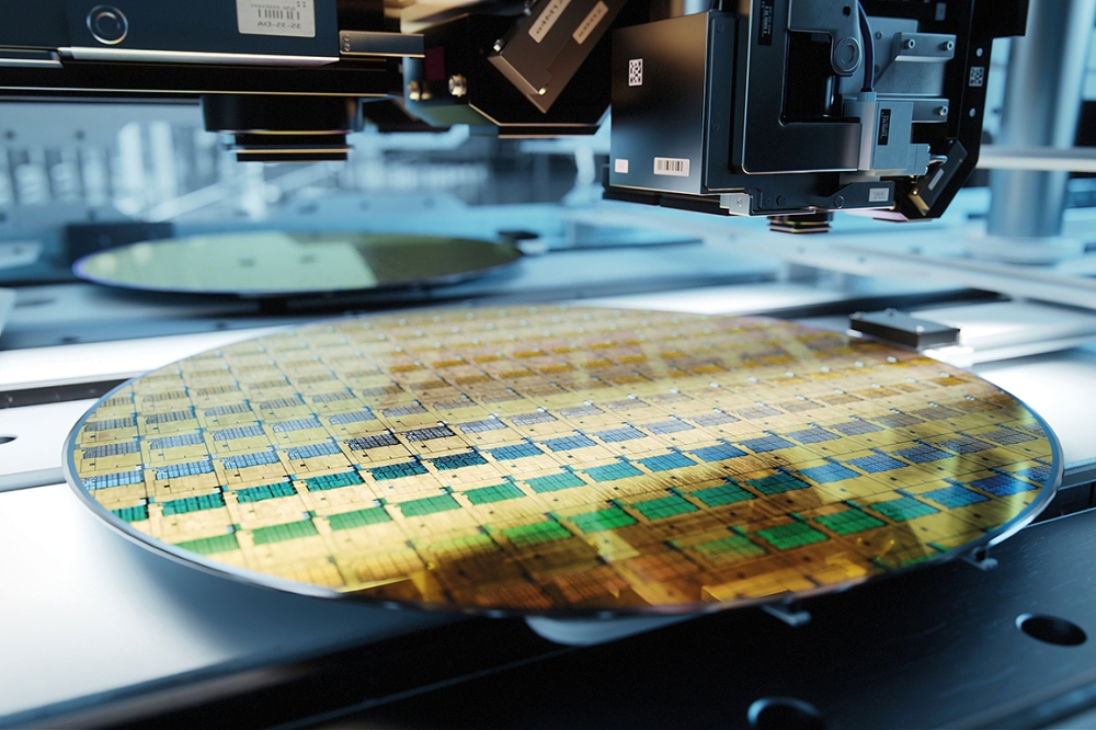
OneChip Photonics is working with Global Communication Semiconductors (GCS), an ISO-certified premier pure-play compound semiconductor wafer foundry.
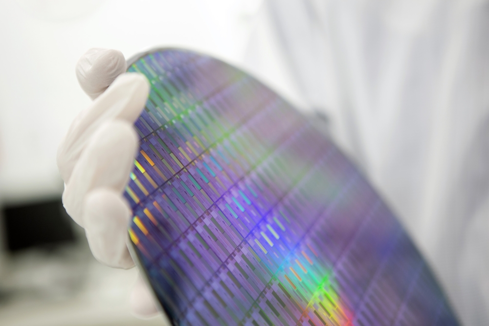
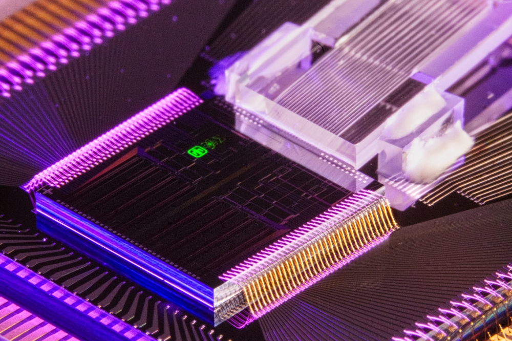
GCS is providing a broad range of InP wafer processing services to OneChip. The firm will use these InP wafers to produce its Photonic Integrated Circuits (PICs) for the Data Centre Interconnect (DCI) and Passive Optical Network (PON) markets.
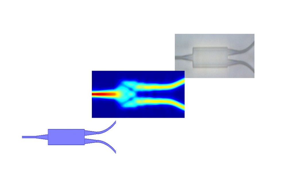
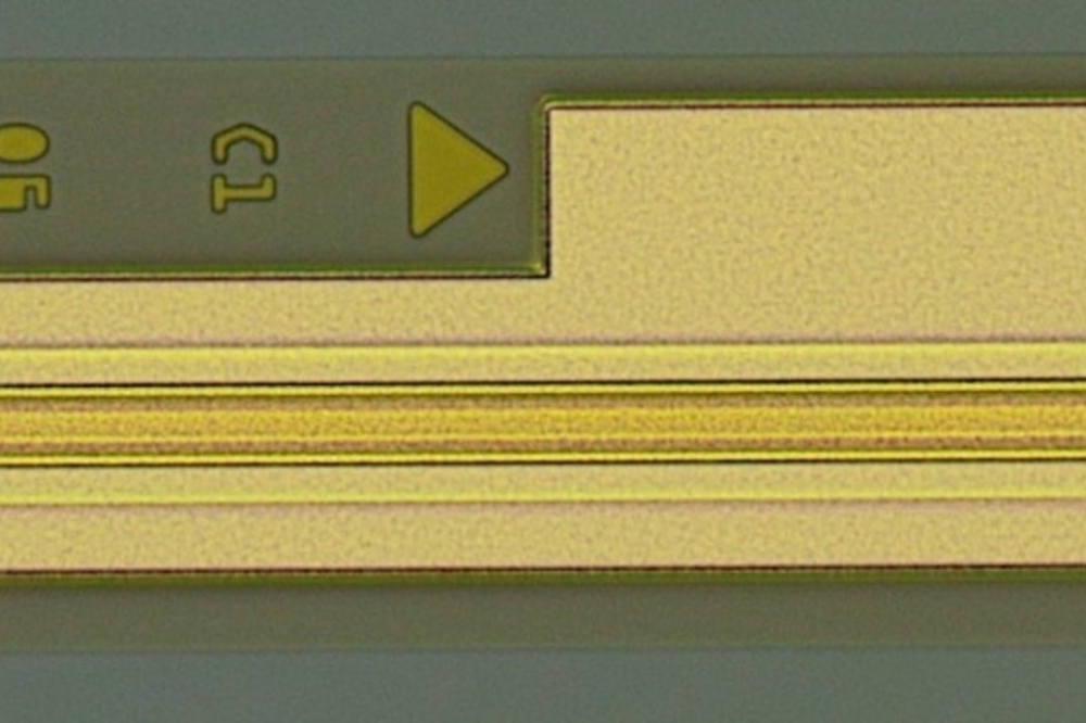
OneChip’s unique, regrowth-free, Multi-Guide Vertical Integration (MGVI) platform eliminates the need for multiple epitaxial growth steps. This enables OneChip to decouple epitaxial growth and wafer processing, while outsourcing both functions to independent, pure-play commercial foundries.
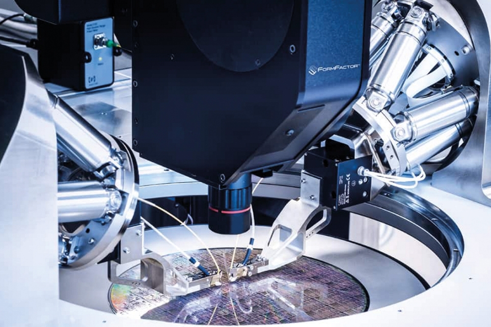
Under this fabless model, OneChip has been working with GCS to process its OneChip-designed 4-inch InP-based wafers. This leverages the infrastructure and expertise GCS has gained through serving high-volume radio frequency (RF) electronics markets.
GCS’s foundry services, based on its Opto and Heterojunction Bipolar Transistor (HBT) processes in InP, are a perfect match to OneChip’s fabless model, which is built around its regrowth-free PIC platform.
What's more, GCS’s Opto and HBT and OneChip’s PIC technologies share the same process and provide a unique Opto-Electronic Integrated Circuit (OEIC) platform. This, for the first time, enables both electronic and photonic integration on one substrate, within the same commercially available fabrication process.
Valery Tolstikhin, Founder and CTO of OneChip Photonics, says, “GCS is the most advanced, pure-play foundry of its kind, which offers Indium Phosphide and high-volume RF electronics processing technologies. Working with GCS gives us the commercial, high-volume processing capability we need to meet the strict cost requirements of the DCI and PON markets.”
Brian Ann, CEO of GCS, adds, “Our InP-based Opto and RFIC process technologies have great synergies with OneChip’s PIC technology. We believe OneChip is a company that can create a truly volume business for photonics in the DCI market, with the unique ability to combine PICs and electronics to create the first optoelectronic circuits in InP.”
OneChip’s regrowth-free, PIC-based InP technology has proven successful in the very cost-sensitive, high-volume PON market, as OneChip’s PIC-based PON transceivers and Bi-directional Optical Sub-Assemblies (BOSAs) already are being deployed by the world’s largest PON system providers.
Now, OneChip is extending this technology to the high-volume DCI market. This market requires 100Gbps+ solutions with higher interface density and longer reach than those within the reach of currently deployed systems in 0.85µm and multi-mode fibres.
The DCI market also requires lower cost and power consumption than the solutions offered by the traditional telecom component vendors.
GCS is an ISO 9001:2008 certified premier pure-play Compound Semiconductor foundry located 15 miles south of Los Angeles International Airport. GCS’s business goal is to supply high performance, high quality, specialty semiconductor devices, integrated circuits and solutions to the wireless, telecommunications and fibre optical communications markets.
In a second collaboration, OneChip is also working with Cardiff based IQE to produce high-volume InP PICs. The company will use IQE’s epitaxial growth services to produce its InP PICs for the DCI and PON markets.
Under this fabless model, OneChip has been working with IQE for the production of its OneChip-designed 4-inch indium phosphide (InP)-based epitaxial wafers. This leverages the infrastructure and expertise IQE has gained over 25 years, supporting the advanced semiconductor industry with its pioneering outsourcing model.
Valery Tolstikhin, Founder and CTO of OneChip Photonics, comments, “The iron-doped, semi-insulating 4-inch InP substrates, and the MOCVD growth technique, required for OneChip’s epi-wafers, are the same as those used by IQE for its high-volume epitaxy products, so we have strong economies of scale in working together. IQE is recognised as a leading independent, pure-play epi-wafer foundry, which not only provides world-class services, but also perfectly fits into our fabless PIC manufacturing model.”
Drew Nelson, President & CEO of IQE, adds, “OneChip has developed some exciting new integrated photonics products for the high-volume, but cost-sensitive, optical communications markets. We are delighted to apply our unique high-volume manufacturing expertise in producing InP-based epi-wafers for OneChip’s innovative PIC technology. OneChip’s use of the fabless manufacturing approach further endorses IQE’s outsourcing business model in the field of photonic devices, and we look forward to helping OneChip continue to scale its business as it extends its unique PIC technology to new markets.”


