Technical Insight
Hybrid silicon prepares to displace InP photonic chips
Will hybrid silicon be the platform of choice for complex photonic integrated circuits? Compound Semiconductor talks to Martijn Heck from the University of California, Santa Barbara, to find out more.

In 2006, researchers at the University of California, Santa Barbara, and Intel unveiled the world's first electrically pumped hybrid silicon laser.
Taking advantage of the light-emitting properties of III-V semiconductors as well as mature CMOS processes to fabricate lasers on a silicon wafer, the device unlocked the door to cheap, mass-produced silicon optical devices.
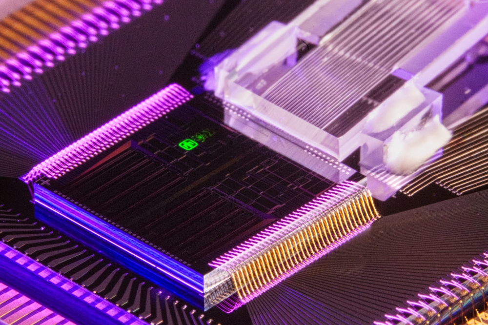
Intel and UCSB unveiled the first hybrid silicon laser in 2006. Credit: Intel
Fast forward seven years and many believe the stage is now well and truly set for a hybrid silicon photonic revolution. Myriad hybrid devices - from laser sources and optical amplifiers to high-speed modulators, waveguides and polarisation components - have been developed, forming the building blocks of photonic integrated circuits (PICs).
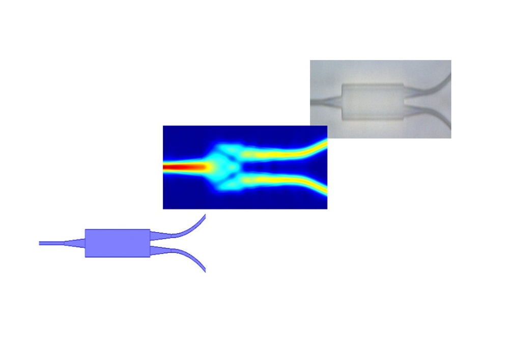
UCSB has developed tapered mode converters to integrate hybrid silicon components with passive silicon-on-insulator substrates and used quantum well intermixing and die-bonding to combine different bandgap components, and devices with different III-V epitaxial stacks.
Across the industry, significant hybrid integrated circuits include highly integrated transmitters, optical phase arrays and optical packet switches. And headline news covers Intel's 50Gbit/s silicon link, Luxtera's 'millionth' chip and Imec fabricating components on 300mm silicon wafers.
With these and other key players, from IBM to UCSB spin-off, Aurrion, hurrying to light up the silicon chip, Martijn Heck from the optoelectronics research groups at UCSB believes today's breakthroughs are just the beginning.
“The promise [of integrating these components] has always been there but we have now increased the yield while specifically looking at performance and processing,” he says. “The cool thing is we can now tie together the components and make these high performance, high functionality photonic integrated circuits.”
This breathtaking rate of progress cannot fail to impress, but InP PICs still very much have the edge. Infinera is currently shipping optical network platforms built using 500Gbit/s PICs, and recently demonstrated a 10Tbit/s PIC. But could this soon change?
Heck and colleagues recently plotted a chart, showing the development of InP and hybrid silicon chip complexity, measured as the number of components per chip.
Development of chip complexity measured as the number of components per chip [credit: MK Smit, JJGM. van der Tol, and MT Hill, "Moore's law in photonics," Laser Photon., vol. 6, no. 1, pp. 1-13, 2012 and MJR Heck et al; “Hybrid Silicon Photonic Integrated Circuit Technology” JSTQE]
Without a doubt, InP-based monolithic integration has increased in complexity exponentially over the past two decades, but according to the researchers, hybrid silicon PICs are catching up, and fast.
Heck believes three key drivers are responsible for the technology's speedy transformation.
“First, we are building on mature III-V technology; we're taking existing knowledge and putting it on a silicon substrate,” he says. “For example we can now fabricate 70GHz modulators, and faster... this shows what a lot of progress we have made with the components.”
Secondly, according to Heck, hybrid-silicon PICs also make use of the mature CMOS fabrication infrastructure for at least part of the process flow. And thirdly, he adds: “Industry adoption has been very quick. Intel, HP and more are working on this and there is a very strong effort in Europe. People recognise the potential for this technology.”
And while the gap between hybrid silicon and InP remains large - tens of components can be integrated on a silicon PIC while hundreds are squeezed onto the InP equivalent - the forthcoming data deluge could drive change. Future terabit-per-second datacom and interconnect applications will demand large volumes of highly integrated PICs. And hybrid silicon with its 300mm silicon substrates and CMOS-compatible fabrication, offers far better economics of scale than the InP-based PIC.
Heck is confident future datacoms and telecoms applications will drive integration of hybrid silicon photonics, and recalls a recent roundtable event, led by UCSB's Institute of Energy Efficiency, that looked at how data centres of tomorrow will cope with data demands.
“All the hot-shots from the main companies [Intel, Cisco, Hewlett Packard and AMD to name but a few] were there and number one on everyone's list was photonics integration ,” he says. “In terms of integration, we all know this is going to scale up. The steps are being taken by Intel and other companies... yes this is slightly speculative, but common sense tells us it will happen.”


