Technical Insight
Outsourcing promises profitable PICs
Metrophotonics' folding in late 2005 was a blessing for one its former employees, Valery Tolstikhin. It encouraged him to try and fulfil his dream of founding a firm with a radically different business model: Using pure-play RF foundries to make optical devices from photonic integrated circuits. Richard Stevenson quizzes him on the details of this vision and the successes to date.
RS: Conventional wisdom decrees that photonic integrated circuits (PICs) must be made in-house to ensure high yields. You have a completely different take on this, don’t you?
Yes. I think that in-house production kills photonic integration, or any other sophisticated component manufacturing for that matter. High yields and low costs only come with appropriate equipment that allows for automated control, quality systems and so on. All of these are only achievable in volumes, and require processes that match the design rules of the fab and the equipment that you deal with.
This is not the case for PICs produced with in-house manufacturing, because, generally speaking, photonics is a very low volume market. It is low on the scale of overall InP production, which is probably about 90 percent RF. So there is no path for any tricks or specific processes to be generalised. So you cannot scale up, and without scaling up you’ll never afford high-end equipment or see standardization and automation leading to cost-yield advantages. That is a vicious circle.
What I tried to do in the very beginning – and this was how the company was found – was to break this circle. My approach was to use standard processes that are available on the market, and preferably, standardize design and fabrication of functional elements of the PICs based on these processes. However, this is only possible when the circuit design is decoupled from the device physics, and design is decoupled from manufacturing. The later requires that you go fabless.
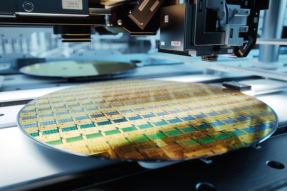
My approach was based on that, and the question was this: Where can I find a big, pure-play foundry to work with? I looked across the board at twelve to fifteen so-called photonic foundries, each contacted directly, and tried to find out what they could and couldn’t do. I came to a very clear conclusion: None of them are really pure-play foundries, in a way one would expect, say, in the silicon IC business. So I turned towards the InP electronic foundries, which have some features of volume scalability, design to manufacturing, autoCAD and the like. It’s not to the extent found in the silicon industry, but it is at least in this direction.
Working with these foundries has one significant sacrifice – you have to give up all the processes that are not part of these foundries. Epitaxial re-growth, for example, is totally excluded, and these foundries don’t have cleave-and-coat because they don’t need this. However, if you manage to go around these issues and reduce the processes to standard etching, passivation, planarization and metallisation steps, you can leverage their cost structure, their tools and their yield control. That’s the path to go for PICs to become an industry, not in-house micro-production.
RS: What is your core technology?
It's an original technology that allows monolithic integration of active and passive devices onto the same substrate in one epitaxial growth step. We do this by vertical stacking of the required materials - all photonic integration is about providing the materials that are right for the function.
We have to use different materials for the detectors and the lasers, and yet combine them on the same substrate. If you don’t use re-growth, the only way you can do this is to stack them up vertically, in a form of vertically integrated functional optical guides. Because of this, we term our re-growth free PIC (photonic integrated circuit) technology as Multi-Guide Vertical Integration (MGVI).
RS: How does your technology differentiate you from most of the component manufacturers in the telecom industry?
Most InP component manufacturers make discrete devices, such as lasers and photodetectors, and package them in TO cans. Other firms then buy them off the shelf and assemble in a photonic circuit. We are different because we don’t do discretes – only PICs. This means that we have a totally different package technology. We have to package an entire PIC with full functionality on it, as opposed to mechanical assembly from discrete parts, which on the active device side are usually pre-packaged in TO cans.
There are also a relatively small number of component manufacturer that do some degree of photonic integration, such as Oclaro and JDSU. The way we are different from those is the technique we use for photonic integration. All our competitors, without exception, use multi-step growth fabrication processes, based on multiple selective etching and re-growth steps. We don’t do this.
RS: How are you different from Infinera, the most famous maker of photonic integrated circuits?
Infinera owns and uses by far the most advanced PIC technology in the world. However, this technology is also probably the most costly and least yielding commercial PIC technology, due to the complexity of the PICs produced. The way these chips are fabricated requires many growth steps.
For Infinera, this doesn’t really matter. It doesn’t sell PICs or components: It only sells systems, and PICs are just a tiny fraction of the cost of the system. Once they have the fab and run three shifts, it works well for them. Whatever the engineers yield, more or less, doesn't really matter because it is still a small cost compared to the cost of the system.
That’s a business model that allowed Infinera to start selling early, because imperfectness of the PICs can be hidden by the system. They have never tried to sell any components, because, for them, it would be cost prohibitive.
We are different in all respects. We sell components, and in certain markets we may sell PICs. We cannot hide that cost into the system, so we do care a great deal about the PIC costs.
RS: Do you do carry out any part of the manufacturing process in-house?
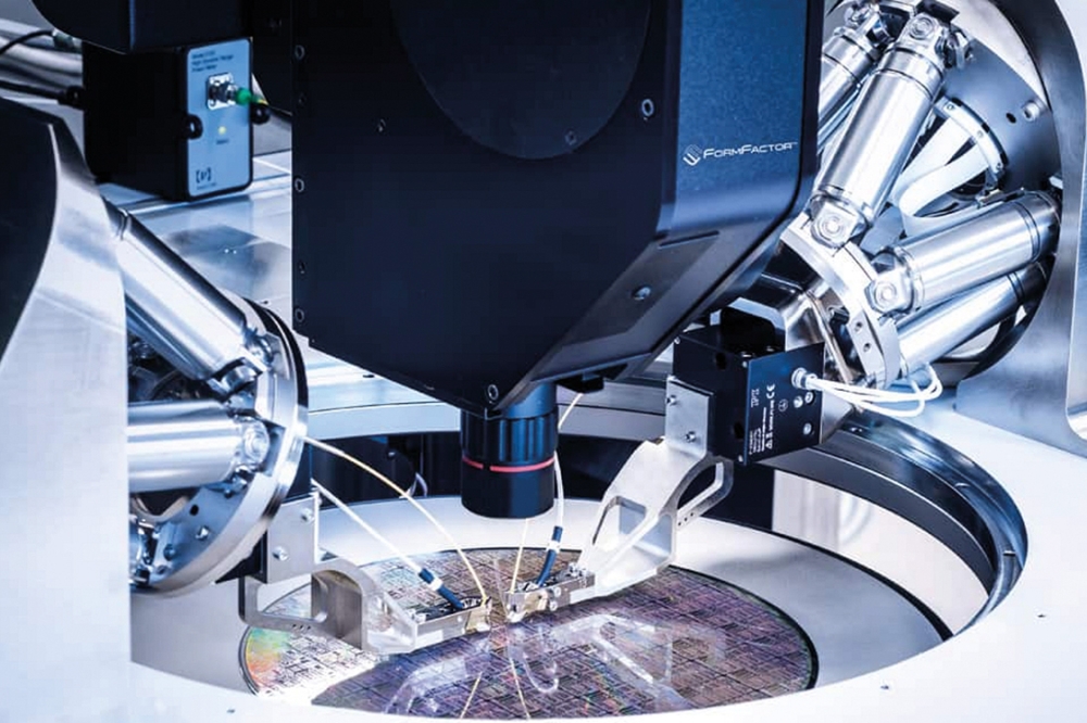
We don’t have production per se in house, but we do have some packaging process development, as well as an extensive test and measurement capability. The package for the PIC is not the same as for the TO-can. It’s not a commodity, so we had to develop some packaging processes in-house before we outsourced them.
RS: Ottawa has a rich history in the photonic business. It was once home to the largest systems company, Nortel, and the largest component company, JDSU. Is it a good place to be based today?
Although Nortel is now defunct, there are a bunch of companies that bought pieces of Nortel and started building up on that. Why is this happening here? There is a talent pool and there is a vibrant Ottawa photonics cluster that stretches from basic research to photonics entrepreneurs. Beside that, the Canadian government provides nice incentives to hi-tech start-ups. Put all this together and it makes good sense to have a business here.
RS: Since the burst of the ‘dot.com’ bubble a decade or so ago, the telecom sector has seen many mergers and little profit. Given this backdrop, how did you mange to win funding to start?
It’s a misconception that investors are shying away from this business simply because it was in a bad shape years ago. They are always looking for a good deal. We had a great idea, an experienced team to implement it, and a very, very attractive market.
RS: What parts of optical network infrastructure are you targeting?
Initially, we started with the ONU [Optical Network Units] sector of the PON market – both Ethernet PON (EPON) and Gigabit PON (GPON). This choice was based on our business model, which required that we choose a market with high volumes and cost-sensitivity.
RS: Talk me through the key features of your go-to-market product?
For FTHH – or say TDM (time-domain multiplexing) PON, which is the biggest slice of this market – we offer PIC-based solutions to ONU transceivers. Currently these are EPON and GPON transceiver modules – a whole module with a pigtail – and also GPON bi-directional optical sub-assemblies (BOSAs).
We have EPON and GPON ONU transceiver modules available now. GPON BOSA is coming a little bit later, but still this year. There is a trend on the market away from a complete module to an on-board BOSA, and we follow this.
RS: One of the biggest selling points of your product is its low manufacturing cost compared to traditional transceivers. How big are the cost savings?
Of course, I cannot give you the numbers since this is a proprietary information. However, think this way. The PON market is a very harsh market and I believe we are the only ones who could put together a PIC-based transceiver for this market. Nobody else could make it for the price.
In addition to the cost saving, our PIC technology provides certain advantages in performance, robustness and footprint size. The PIC itself offers a huge advantage in overall photonic circuit stability by eliminating any moving parts. Then, our specific PIC platform, MGVI, offers best-in-class performance, or at least state-of-the-art solutions, for many key elements of the PIC, like spot-size converters and waveguide photodetectors. We have some advantages in the mode stability of the lasers because of the platform we use, too. This translates into good customer traction.
RS: How much investment has OneChip netted so far, and when do you expect to hit profitability?
We have raised above $60 million, and we will need more for production-capacity-build-up, which is coming. I believe we will be a profitable venture by the end of 2013, with an accuracy of a quarter or so.
RS: The company is now in its sixth year, and it is only just starting to sample its first product. That seems like a long time to go to market. Is that a fair criticism?
It depends on your perspective. We don’t assemble the parts made by others, and we don’t use investors’ cash to buy equipment to make the things that other people do. We have developed a brand new technology, and this is intimately related to the brand new business model. So it takes time, especially given that our initial products are modules, not just PICs, and hence required an adequate packaging technology to be developed as well. It’s not PICs that we sell - we had PICs ready a couple of years before we started sampling the modules. All the rest takes time as well.
Let me give you a few examples, so you can compare our progress to that of others. Infinera started in 2000 and they announced the first digital node product featuring their PICs in about 2006, so it took them about six years [to bring their first product to market], despite an investment of above $300 million.
In a different world, silicon photonics, the most prominent company today is Luxtera. They started in 2001 and sold their first active optical cables – essentially a pair of optical transceivers with a piece of fibre between them – around 2009. Luxtera are a bit like us, because they are fabless and have worked with a commercial CMOS foundry.

Figure 1. The manufacturing process flow employed by OneChip Photonics for the production of its first product, which targets the Optical Network Unit market.
RS: Do you expect the telecom components market to pick up?
The telecom component market doesn’t seem to have great capacity to grow, apart from the access market. But if you add on the data-com market, that’s a totally different picture. We see huge potential in the datacom market, driven by social media rise that skyrocketed demand for bandwidth and data storage/processing, which eventually will result in the datacom surpassing telecom by far.
RS: How will your product portfolio expand over the coming years?
Over the last five years we have extensively been in development. It’s not just the PON product, but generic PIC technology development. This is based on a number of unique things, like the separation of growth and processing, and separation of device and circuit design.
The latter allows re-use of the once-developed building blocks, which are devices with a certain specific functionality, such as lasers or detectors. This is the key to our product portfolio. We take those building blocks and re-use them with very little modification – not changing basic design, process, or things like that – to other applications.
What are these other applications that we are looking at? We want massive markets with cost sensitivity, so we have started looking at optical interconnect markets for datacom, because they are driven by the same cost – volume dynamics as the PON market. We have in the pipeline, in different stages, 40 G coarse WDM for QFSP and QFSP+ packages and 100G LAN WDM for data centre interconnects. Also, we have space division multiplexing solutions for 40G and 100G optical interconnects, phase and polarization division multiplexing for 100G coherent and various combinations of all multiplexing techniques I have described for expanding our portfolio well beyond 100G. We have all that in different stages of development, with a roadmap taking us to 1 Terabit. Overall the markets we address are in the multi-billion dollar range.
RS: How many products do you expect to sell over the next few years?
It depends what you mean by product. Some people change the socket and call it a different product. We identify market areas.
There is definitely a PON market in which we will continue to build up, so we have more products to offer to them. This market is very healthy, and growing steadily.
We also see a huge opportunity in optical interconnects. This is a very wide area, and we only target the sectors that require a fibre and propagation over a few hundred metres. So it’s not chip-to-chip. It’s single-mode fibre, with all kinds of multiplexing – space, wavelength, phase and polarization.

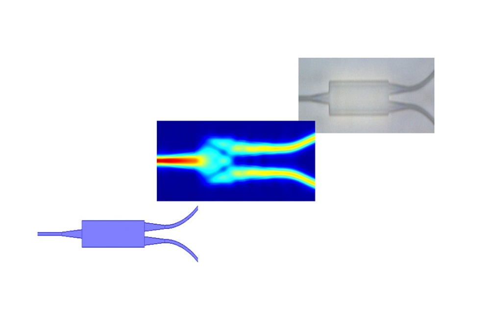
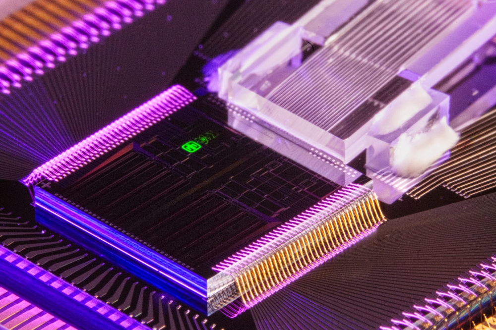
Figure 2. In May 2012 OneChip Photonics released its 4 x 25(28)G LAN WDM receiver PICs, which are now being trialled by tier I customers. Each of these products combines: A spot-size converter for efficient, alignment-tolerant fibre-coupling; a WDM section, either in the form of arrayed waveguide grating or a diffractive echelle grating; and an array of waveguide photodetectors inserted in the output waveguides of the WDM unit.
RS: You have selected Fabrinet for your contract manufacturing. Why did you choose them, and are they your only partner?
We looked at many companies before selecting Fabrinet. For the time being, and given the product of today, we choose Fabrinet as the number one, based on cost-to-value. That fits today’s assembly needs. However, we also have agreements with Sanmina SCI, and we are on the lookout for new partners. Fabrinet works for us very well now, but we are not locked in with them forever. For epi and wafer processing we use separate, big commercial foundries.
RS: Will your manufacturing partners be able to cope with this ramp in production volumes?
Yes. The manufacturing model based on PICs is very scalable. You don’t have to hire and train new assemblers – you just add more wafers. There are no limits here. Even if we have the lion’s share of the telecom and data-com markets, this will be a small fraction of InP production for RF. So even with existing manufacturing capabilities we are very well placed.

Valery Tolstikhin, Founder and CTO of OneChip Photonics, has been involved in research and commercialization of advanced semiconductor devices for micro- and optoelectronics since completion his Ph.D. in 1980. His work in photonic integration started in late nineties and includes development of new integration platform, novel integrated photonic devices and original PICs in InP. Tolstikhin is an adjunct professor at University of Ottawa.
Yes. I think that in-house production kills photonic integration, or any other sophisticated component manufacturing for that matter. High yields and low costs only come with appropriate equipment that allows for automated control, quality systems and so on. All of these are only achievable in volumes, and require processes that match the design rules of the fab and the equipment that you deal with.
This is not the case for PICs produced with in-house manufacturing, because, generally speaking, photonics is a very low volume market. It is low on the scale of overall InP production, which is probably about 90 percent RF. So there is no path for any tricks or specific processes to be generalised. So you cannot scale up, and without scaling up you’ll never afford high-end equipment or see standardization and automation leading to cost-yield advantages. That is a vicious circle.
What I tried to do in the very beginning – and this was how the company was found – was to break this circle. My approach was to use standard processes that are available on the market, and preferably, standardize design and fabrication of functional elements of the PICs based on these processes. However, this is only possible when the circuit design is decoupled from the device physics, and design is decoupled from manufacturing. The later requires that you go fabless.
My approach was based on that, and the question was this: Where can I find a big, pure-play foundry to work with? I looked across the board at twelve to fifteen so-called photonic foundries, each contacted directly, and tried to find out what they could and couldn’t do. I came to a very clear conclusion: None of them are really pure-play foundries, in a way one would expect, say, in the silicon IC business. So I turned towards the InP electronic foundries, which have some features of volume scalability, design to manufacturing, autoCAD and the like. It’s not to the extent found in the silicon industry, but it is at least in this direction.
Working with these foundries has one significant sacrifice – you have to give up all the processes that are not part of these foundries. Epitaxial re-growth, for example, is totally excluded, and these foundries don’t have cleave-and-coat because they don’t need this. However, if you manage to go around these issues and reduce the processes to standard etching, passivation, planarization and metallisation steps, you can leverage their cost structure, their tools and their yield control. That’s the path to go for PICs to become an industry, not in-house micro-production.
RS: What is your core technology?
It's an original technology that allows monolithic integration of active and passive devices onto the same substrate in one epitaxial growth step. We do this by vertical stacking of the required materials - all photonic integration is about providing the materials that are right for the function.
We have to use different materials for the detectors and the lasers, and yet combine them on the same substrate. If you don’t use re-growth, the only way you can do this is to stack them up vertically, in a form of vertically integrated functional optical guides. Because of this, we term our re-growth free PIC (photonic integrated circuit) technology as Multi-Guide Vertical Integration (MGVI).
RS: How does your technology differentiate you from most of the component manufacturers in the telecom industry?
Most InP component manufacturers make discrete devices, such as lasers and photodetectors, and package them in TO cans. Other firms then buy them off the shelf and assemble in a photonic circuit. We are different because we don’t do discretes – only PICs. This means that we have a totally different package technology. We have to package an entire PIC with full functionality on it, as opposed to mechanical assembly from discrete parts, which on the active device side are usually pre-packaged in TO cans.
There are also a relatively small number of component manufacturer that do some degree of photonic integration, such as Oclaro and JDSU. The way we are different from those is the technique we use for photonic integration. All our competitors, without exception, use multi-step growth fabrication processes, based on multiple selective etching and re-growth steps. We don’t do this.
RS: How are you different from Infinera, the most famous maker of photonic integrated circuits?
Infinera owns and uses by far the most advanced PIC technology in the world. However, this technology is also probably the most costly and least yielding commercial PIC technology, due to the complexity of the PICs produced. The way these chips are fabricated requires many growth steps.
For Infinera, this doesn’t really matter. It doesn’t sell PICs or components: It only sells systems, and PICs are just a tiny fraction of the cost of the system. Once they have the fab and run three shifts, it works well for them. Whatever the engineers yield, more or less, doesn't really matter because it is still a small cost compared to the cost of the system.
That’s a business model that allowed Infinera to start selling early, because imperfectness of the PICs can be hidden by the system. They have never tried to sell any components, because, for them, it would be cost prohibitive.
We are different in all respects. We sell components, and in certain markets we may sell PICs. We cannot hide that cost into the system, so we do care a great deal about the PIC costs.
RS: Do you do carry out any part of the manufacturing process in-house?
We don’t have production per se in house, but we do have some packaging process development, as well as an extensive test and measurement capability. The package for the PIC is not the same as for the TO-can. It’s not a commodity, so we had to develop some packaging processes in-house before we outsourced them.
RS: Ottawa has a rich history in the photonic business. It was once home to the largest systems company, Nortel, and the largest component company, JDSU. Is it a good place to be based today?
Although Nortel is now defunct, there are a bunch of companies that bought pieces of Nortel and started building up on that. Why is this happening here? There is a talent pool and there is a vibrant Ottawa photonics cluster that stretches from basic research to photonics entrepreneurs. Beside that, the Canadian government provides nice incentives to hi-tech start-ups. Put all this together and it makes good sense to have a business here.
RS: Since the burst of the ‘dot.com’ bubble a decade or so ago, the telecom sector has seen many mergers and little profit. Given this backdrop, how did you mange to win funding to start?
It’s a misconception that investors are shying away from this business simply because it was in a bad shape years ago. They are always looking for a good deal. We had a great idea, an experienced team to implement it, and a very, very attractive market.
RS: What parts of optical network infrastructure are you targeting?
Initially, we started with the ONU [Optical Network Units] sector of the PON market – both Ethernet PON (EPON) and Gigabit PON (GPON). This choice was based on our business model, which required that we choose a market with high volumes and cost-sensitivity.
RS: Talk me through the key features of your go-to-market product?
For FTHH – or say TDM (time-domain multiplexing) PON, which is the biggest slice of this market – we offer PIC-based solutions to ONU transceivers. Currently these are EPON and GPON transceiver modules – a whole module with a pigtail – and also GPON bi-directional optical sub-assemblies (BOSAs).
We have EPON and GPON ONU transceiver modules available now. GPON BOSA is coming a little bit later, but still this year. There is a trend on the market away from a complete module to an on-board BOSA, and we follow this.
RS: One of the biggest selling points of your product is its low manufacturing cost compared to traditional transceivers. How big are the cost savings?
Of course, I cannot give you the numbers since this is a proprietary information. However, think this way. The PON market is a very harsh market and I believe we are the only ones who could put together a PIC-based transceiver for this market. Nobody else could make it for the price.
In addition to the cost saving, our PIC technology provides certain advantages in performance, robustness and footprint size. The PIC itself offers a huge advantage in overall photonic circuit stability by eliminating any moving parts. Then, our specific PIC platform, MGVI, offers best-in-class performance, or at least state-of-the-art solutions, for many key elements of the PIC, like spot-size converters and waveguide photodetectors. We have some advantages in the mode stability of the lasers because of the platform we use, too. This translates into good customer traction.
RS: How much investment has OneChip netted so far, and when do you expect to hit profitability?
We have raised above $60 million, and we will need more for production-capacity-build-up, which is coming. I believe we will be a profitable venture by the end of 2013, with an accuracy of a quarter or so.
RS: The company is now in its sixth year, and it is only just starting to sample its first product. That seems like a long time to go to market. Is that a fair criticism?
It depends on your perspective. We don’t assemble the parts made by others, and we don’t use investors’ cash to buy equipment to make the things that other people do. We have developed a brand new technology, and this is intimately related to the brand new business model. So it takes time, especially given that our initial products are modules, not just PICs, and hence required an adequate packaging technology to be developed as well. It’s not PICs that we sell - we had PICs ready a couple of years before we started sampling the modules. All the rest takes time as well.
Let me give you a few examples, so you can compare our progress to that of others. Infinera started in 2000 and they announced the first digital node product featuring their PICs in about 2006, so it took them about six years [to bring their first product to market], despite an investment of above $300 million.
In a different world, silicon photonics, the most prominent company today is Luxtera. They started in 2001 and sold their first active optical cables – essentially a pair of optical transceivers with a piece of fibre between them – around 2009. Luxtera are a bit like us, because they are fabless and have worked with a commercial CMOS foundry.

Figure 1. The manufacturing process flow employed by OneChip Photonics for the production of its first product, which targets the Optical Network Unit market.
RS: Do you expect the telecom components market to pick up?
The telecom component market doesn’t seem to have great capacity to grow, apart from the access market. But if you add on the data-com market, that’s a totally different picture. We see huge potential in the datacom market, driven by social media rise that skyrocketed demand for bandwidth and data storage/processing, which eventually will result in the datacom surpassing telecom by far.
RS: How will your product portfolio expand over the coming years?
Over the last five years we have extensively been in development. It’s not just the PON product, but generic PIC technology development. This is based on a number of unique things, like the separation of growth and processing, and separation of device and circuit design.
The latter allows re-use of the once-developed building blocks, which are devices with a certain specific functionality, such as lasers or detectors. This is the key to our product portfolio. We take those building blocks and re-use them with very little modification – not changing basic design, process, or things like that – to other applications.
What are these other applications that we are looking at? We want massive markets with cost sensitivity, so we have started looking at optical interconnect markets for datacom, because they are driven by the same cost – volume dynamics as the PON market. We have in the pipeline, in different stages, 40 G coarse WDM for QFSP and QFSP+ packages and 100G LAN WDM for data centre interconnects. Also, we have space division multiplexing solutions for 40G and 100G optical interconnects, phase and polarization division multiplexing for 100G coherent and various combinations of all multiplexing techniques I have described for expanding our portfolio well beyond 100G. We have all that in different stages of development, with a roadmap taking us to 1 Terabit. Overall the markets we address are in the multi-billion dollar range.
RS: How many products do you expect to sell over the next few years?
It depends what you mean by product. Some people change the socket and call it a different product. We identify market areas.
There is definitely a PON market in which we will continue to build up, so we have more products to offer to them. This market is very healthy, and growing steadily.
We also see a huge opportunity in optical interconnects. This is a very wide area, and we only target the sectors that require a fibre and propagation over a few hundred metres. So it’s not chip-to-chip. It’s single-mode fibre, with all kinds of multiplexing – space, wavelength, phase and polarization.

Figure 2. In May 2012 OneChip Photonics released its 4 x 25(28)G LAN WDM receiver PICs, which are now being trialled by tier I customers. Each of these products combines: A spot-size converter for efficient, alignment-tolerant fibre-coupling; a WDM section, either in the form of arrayed waveguide grating or a diffractive echelle grating; and an array of waveguide photodetectors inserted in the output waveguides of the WDM unit.
RS: You have selected Fabrinet for your contract manufacturing. Why did you choose them, and are they your only partner?
We looked at many companies before selecting Fabrinet. For the time being, and given the product of today, we choose Fabrinet as the number one, based on cost-to-value. That fits today’s assembly needs. However, we also have agreements with Sanmina SCI, and we are on the lookout for new partners. Fabrinet works for us very well now, but we are not locked in with them forever. For epi and wafer processing we use separate, big commercial foundries.
RS: Will your manufacturing partners be able to cope with this ramp in production volumes?
Yes. The manufacturing model based on PICs is very scalable. You don’t have to hire and train new assemblers – you just add more wafers. There are no limits here. Even if we have the lion’s share of the telecom and data-com markets, this will be a small fraction of InP production for RF. So even with existing manufacturing capabilities we are very well placed.

Valery Tolstikhin, Founder and CTO of OneChip Photonics, has been involved in research and commercialization of advanced semiconductor devices for micro- and optoelectronics since completion his Ph.D. in 1980. His work in photonic integration started in late nineties and includes development of new integration platform, novel integrated photonic devices and original PICs in InP. Tolstikhin is an adjunct professor at University of Ottawa.


