Europe backs a central foundry for photonic integrated circuits

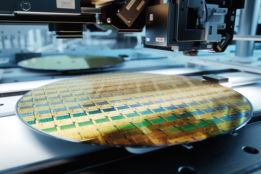
Q Explain the motivation for creating a European foundry for InP photonic integrated circuits? A MS: What we’re trying to do is introduce into InPbased photonics a similar foundry model to that which is so successful in CMOS microelectronics. I think it’s good to distinguish between what we call custom foundries and generic foundries. A lot of fabs that call themselves foundries offer to develop a process for you, but with generic foundries, the process is standardized. That’s new and it makes access to this PIC technology much easier and cheaper. There are two institutes that already offer that kind of foundry service on a research basis: ePIXfab for silicon photonics; and JePPIX (Joint European Platform for InPbased Photonic Integrated Components and Circuits) for InP. What we are talking about here is transferring the JePPIX approach into industry. Hopefully a European PIC foundry will exist in 2013. Q The millions and millions of dollars poured into PIC technology have not provided a great return on investment. How will the European manufacturing platform for photonic integrated circuits (EuroPIC) change that? A DR: Actually, the technology in these types of photonic integrated circuits is having quite a lot of commercial success. But this is only in the telecoms arena, where there is enough money and drive to deliver the integration needed to make those systems work. One issue is that by and large the equipment suppliers in the telecoms, which are very dedicated in their own narrow commercial structures, don’t give access to their fabs. However, even if they did, the cost of development of the chips for someone else would be pretty horrendous. Even custom fabs, which operate at a lower cost level, are pretty expensive. If we can develop along generic lines, PICs can become much cheaper - maybe one or two orders of magnitude cheaper. From there we can start to grow the market volumes in other sectors. MS: Another important point is that once you have the platform technology and a lot of companies are using it, it will be worth the effort of creating a dedicated design kit and component library. Once you have that, you will design to accurate models, speeding up the whole design process and making it more accurate. That’s what has happened in microelectronics. Photonics technology is much too fragmented, with design software at a very basic level compared to the electronics industry. Q Once the foundry is up and running, who will be its main users? A MS: They will be University spin-offs and SMEs that want to investigate the application of PICs in novel or improved products, and also larger companies that can develop their PICs at significantly lower costs. We have a list of fifty companies, our user group, with potential interest in this generic approach. The target is to increase that to at least one hundred within two years. DR: The strength of the EuroPIC approach is that companies can get a handful of chips relatively cheaply and quickly. If they end up wanting many wafers a year, the same plants can produce that volume as well, because all processes are carried out using industrial facilities capable of high-volume production. Q Why will SMEs have a better chance of success by working with EuroPIC? A DR: Any fabs would find it extremely difficult to work with large numbers of SMEs. You really need some kind of independent expertise in between the fabs and the applications: people to organize the whole process; people to do the design. The companies with the fabs do not have the manpower available. However, it is true that if a company was ramping its production to high volumes, it would be worth its while to talk directly with a fab, but we are talking about the companies starting in low volume. The photonics industry has thinned down a lot since the dot.com boom-and bust at the turn of the century, and very few of the big players who are left have the spare capacity to take on this work. Q Will the EuroPIC foundries help companies to speed products to market? A DR: Yes. You can imagine a small SME with half a dozen people trying to sort everything out for themselves and struggling to get anywhere. When you have this infrastructure available, rapid prototyping becomes a reality. You will be able to go from an idea to having a chip in your hands in a few months. It will be incredibly different to the position we have now. Q Do you think that Europe lags the US and Asia, in terms of PIC development and commercialization? A MS: Europe had the lead in photonic integration in the 1990s. However, after the turn of the century US companies, such as Infinera, came up very rapidly. However, in this novel approach - the generic technology - Europe has a lead. Something like this is not happening in the US or Japan. To succeed you need two things: a consortium that is very closely co-operating, which we have in Europe; and substantial supporting funding. Q Where does the European foundry stand today? A DR: It’s at an R&D level. The University of Eindhoven is supporting the JePPIX operation, which runs an R&D generic line on its open facility. What we are trying to do is to move that understanding and capability out into industry, where you can get all the good things like volume, reliability, throughput. To do this, EuroPIC is working with Oclaro in the UK and HHI (Heinrich Hertz Institute) in Berlin. Philips is also playing a role, although it is a little bit behind those to two foundries. Although Oclaro’s technology is not advertised as largescale photonic integrated circuits in quite the way Infinera’s technology is, it is every bit the equal of it. It can do very similar things, but Oclaro has chosen until now to apply it specifically to tunable lasers, modulators, and so on. Q What are the benefits for Oclaro and HHI, the key foundries in the EuroPIC project? A DR: They are both fabs with a telecom base with a huge amount of highly sophisticated technology firmly directed in one narrow application area. They would both like to see their technological abilities more broadly deployed. Q Tell me about the progress of EuroPIC? A DR: It started on 1st August last year, and it’s a relatively long cycle time to get the first generic line set up. We have spent a year putting existing and new pieces together in the process phase, and we are just about to start our first runs at the InP processing facilities. EuroPIC will aim to go through this cycle twice, in order to iron out difficulties. MS: What has been achieved now is mainly coming from the JePPIX platform. This is research, but within two to three years we hope to bring this to an industrial level. We have selected ten different applications [see box “PIC applications” for details], and they will all be put on the two foundry lines. By the middle of next year we should have one set of wafers from each of the foundries, each wafer having a lot of quite different chips integrated on it. Q Are the foundries continuing to refine their technology? A DR: Very much so. Although to be honest, EuroPIC is a very broad, SME-based program, and there’s not that much space for developing a radically new semiconductor technology. The novelty in the program is largely to do with putting end-to-end process together, but there will be new technologies in packaging and software. However, the platform is capable of considerable development in terms of the semiconductor technology that goes into it, because there are a lot of different InP alloys that you can use. There is the whole area of quantum dots and nanotechnology, which we could go into in the future. Q What wavelengths will these PICs operate at? A MS: Initially the telecom C-band (around 1550 nm), but the platform is capable of extension. Q Are there facilities to package these chips? A DR: Our packaging effort is rather small. There is a resource limitation – EuroPIC is a € 6 million program. We have one partner who is beginning to look at the prospects of a generic packaging technology, CIP Technologies in the UK. We are also starting new programs, where packaging is a very large part of the activity. MS: Our process is standardized on the interface electrically and optically, so that you can use the same package for a lot of different chips. We can see that the chip price may go down by a factor of more than ten. If the cost of packaging is not to become the bottleneck, it will have to go down too, which basically means cutting the cost of alignment using leading edge packaging technologies; ‘clip-it-together’ and ‘plug-and-play’ techniques. Q Do companies need to be worried about compromising IP if they work with EuroPIC? A DR: We have drawn up non-disclosure agreement so we can work with our user group. In the future we may have a brokering organization sitting between the application and the InP fab. Contracts between the broker and the fab, and the broker and the application holders can sew up IP in a completely watertight fashion. Q How will SMEs work with the European PIC foundry to develop products and bring them to market? A MS: If they have sufficient expertise in-house they can design their mask set. But we expect that most companies will not have that expertise, so we are also working on the creation of design houses to generate designs, just as you have design houses in microelectronics. Q How is the foundry funded at the moment? A MS: Essentially European and national funding, with some matching funding from industry, depending on the scheme. The COBRA research school at TU/e is underwriting JePPIX next year. COBRA runs training courses based in the university’s electrical engineering department on the design of the overall technology, and it occasionally offers multi-project wafer runs. In the Netherlands we have the so-called Memphis (Merging Electronics and Micro & Nano-Photonics for Integrated Circuits) Smart Mix project. It’s a big and rather broad program, but there is substantial funding for this generic approach. There is another program in the Netherlands: the STW Perpectief program GTIP, worth € 5.5 million, which is fully devoted to generic integration technologies. It will start at the end of this year. DR: There is also PARADIGM (Photonic Adavanced Manufacturing Platform for Photonic Integrated Circuits), another EU project under negotiation, which will hopefully start in the early autumn. It can be viewed as a successor to EuroPIC. Paradigm will focus on technology developments, such as packaging and InP processing technologies. Assuming that Paradigm is funded, we will then have € 20-30 million going into this area, spread over about twenty five different companies. This gives you a critical mass to make you feel that you can make a central European InP foundry a reality. Q Given all the talk about austerity measures by the governments of many European countries, are you concerned over future funding of EuroPIC? A MS: This technology will make product development much cheaper, which must be a good message in the current climate. For the coming two-to-three years foundry based R&D will be in a good position with secured funding. The critical point is this: will the commercial market for low-cost PICs grow fast enough? DR: I would add that these austerity measures by the European governments are not over everything. Governments are trying to cut their government expenditure and stimulate their industries, and we are one of the industries that can stimulate growth.


