Unlocking the Value of Fab Ownership
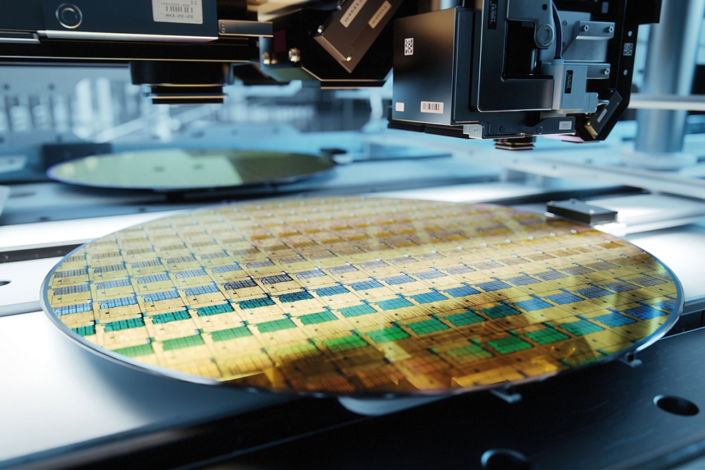
Fab or Fabless? The question has been asked many times over the last ten years by everyone seeking to make compound semiconductor optoelectronic devices. There is no doubt that the era has passed when the first item on a start-up shopping list was a fabrication facility....but what about companies with well established fabs, such as Oclaro? Are their fabs cash and overhead drains, or are they the key to deliver growth and profitability now that the market is warming up and many component requirements are still differentiated on performance and footprint? The view of the management at Oclaro is that fab ownership offers compelling advantages, and once a certain scale is reached, it is highly differentiating and cost effective. In addition, it acts as a significant barrier to entry for other players.
![]()
Why have a fab?...
Owning a fabrication facility is expensive, and significant volume and scale are needed to allow cost recovery and profitability. Many companies have sought ways of reducing this overhead by outsourcing fabrication, giving quick benefits to the bottom line. However, several aspects of the industry are now changing, and we believe this alters the balance significantly.
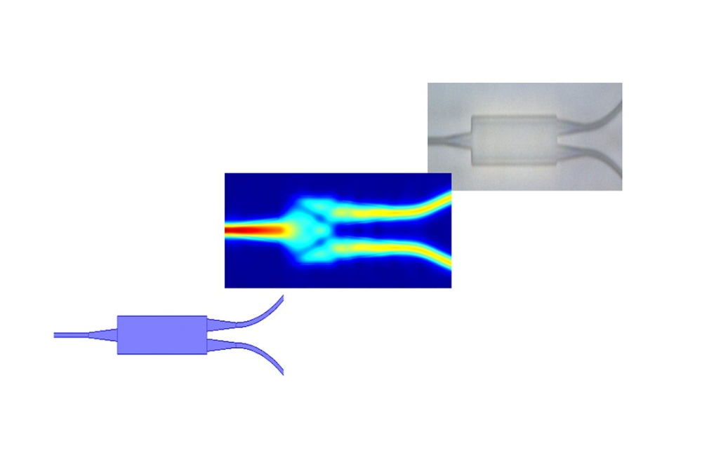
There has been and continues to be consolidation, so fewer players are driving higher volumes through their facilities. In addition, many applications are demanding significant levels of photonic integration – not necessarily large scale multi-channel photonic integrated circuits (PICs), but integration of a number of elements, such as lasers, monitor detectors and modulators to drive down footprint and cost whilst delivering best in class performance at the right module level cost point. Component companies seek differentiation in cost, performance and time to market. Ownership of a fab must enable all three aspects to be of full benefit. Time to market benefits can be achieved through utilisation of common and verified building blocks and processes with which devices are built. This is increasingly important, as higher levels of integration are required to meet the functionality demanded.
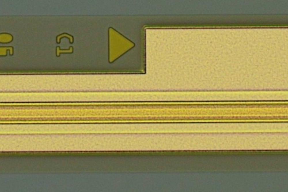
At Oclaro, we have adopted such an approach to integration. We utilse multiple ‘etch and regrowth’ processes to fabricate components – three in the case of a tunable laser and five for integrated laser modulators. Such an approach to device fabrication is often targeted for avoidance by outsource advocates, due to complexity and yield issues, whereas our investment in processes and procedures, such as regrowth initiation and surface cleaning, ensure that yield is maintained even for the most complex processes.
An advantage of such an approach is that no compromise need be built in to the actual design – the best semiconductor structure can still be independently used for a waveguide, laser active region and modulator. We believe this compares very favourably with the alternatives, which use processes such as QWI (Quantum Well Intermixing) or vertically coupled waveguide structures to achieve multi-element functionality. The ‘etch and regrowth’ methodology gives virtually complete flexibility in design, as well as allowing smooth introduction of improved processes.
Large compound semiconductor fab. costs are typically several million dollars per quarter, so it is useful to ask at what level the fab becomes ‘profitable’ to the company. A reasonable ‘rule of thumb’ might be when the fab supports revenue of five to ten times the overhead cost, but as the level of functionality at the chip level is enhanced, the effective ‘value’ of the chip within the product significantly increases.
For the latest generations of components, such as tunable transmitters , the costs are already favourable, and set to become increasingly so. We are now getting to the point where the incremental cost of the chip fabrication is becoming dominated by materials and direct labour rather than overhead.
There are perceived advantages to outsourcing in some areas, such as process flexibility, as foundries must support different processes and materials for a wide range of customers. Initial entry costs are low, and capital requirements for the user are minimal. Many of the problems – such as design and IP protection can be managed, provided appropriate controls and procedures are put in place.
The outsource model requires more emphasis on design IP, whereas insourcing enables more leverage from process IP and knowledge. For low volume and start ups, outsourcing is attractive; the barriers come in scaling this to global volume requirements the industry demands.
![]()
![]()
Oclaro fabs....
Oclaro owns a number of fabrication sites, including facilities for Lithium Niobate, Thin Film filters, Liquid Crystal (as part of the recent Xtellus WSS acquisition) and two major compound semiconductor fabs, at Zurich, Switzerland, and Caswell in the UK.
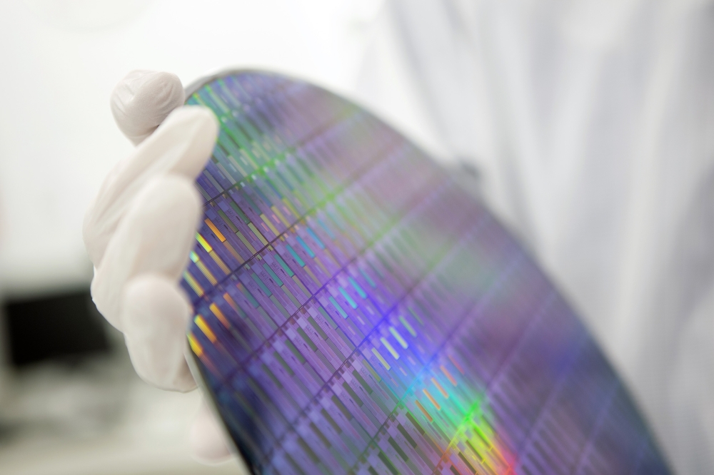
The two compound semiconductor facilities differentiate in the materials and applications: the Zurich facility is used for the fabrication of high power pump and industrial lasers as well as VCSELs based on GaAs; the Caswell facility focuses mainly on InP based devices as well as providing additional capacity for industrial lasers. Base material growth is by MBE exclusively for pump lasers (Zurich) and by MOCVD (InP and GaAs) at Caswell.
The other Oclaro fabrication facilities are somewhat smaller scale, more specialist and largely independent of the two major fabs, except in aspects of management and best practice sharing. The availability of both InP based and Lithium Niobate (LN) modulator technologies within Oclaro is advantageous and cost effective, with the LN devices appealing as a ‘component’ play wheras InP is very attractive as an integration platform and for PICs. The process complexity of the GaAs based lasers is relatively low compared to that for the InP based devices and circuits, so the article here will focus on the latter, particularly with reference to the more complex integrated devices that are manufactured.
Needs and Differentiators...
Critical to unlocking the value of fab ownership is deciding what the device and circuit demand might be. Our transmission business primarily concentrates on the DWDM space, for long haul and Metro applications.
Bandwidth demand continues to grow exponentially, with steadily reducing revenue per bit. Key attributes of the emerging infrastructure include: packet friendly common infrastructure; converged voice, data & video; zero touch service provision; lower operating costs; node consolidation; scalable service speeds; scalable service level agreements; and increased capacity.
![]()
Taking all these together we see a trend to the implementation of an intelligent photonic core, with a reconfigurable optical add-drop multiplexer (ROADM) interconnected mesh topology; full band tunability is critical, with primary capacity per wavelength increasing from 10 to 40 and 100Gbps. More complex modulation formats, including RZ-DQPSK at 40Gbps and coherent PM-QPSK for 100Gbps are increasingly required to allow for upgrades to existing 10Gbps routes using install fibre plant and to cost reduce new build by transferring dispersion management from the optical domain into the electronic using DSP and coherent detection.
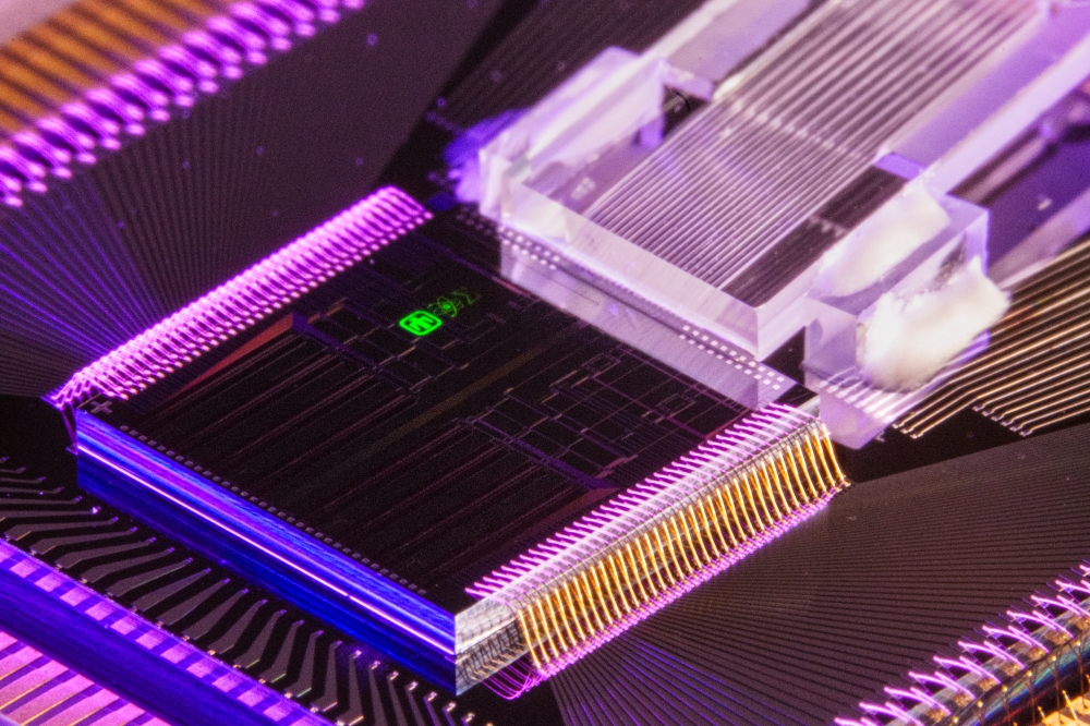
For all these requirements, photonic integration is a key enabling technology for cost and footprint reduction. The challenge is to ‘print’ the complexity through photonic integration and achieve the scalability through batch processing of wafers. Moving further towards the edges of the network, low cost provisioning of 10G DWDM tunable links in as small a form factor as possible – XFP, SFP+ and pluggable multichannel will be increasingly important. Again, photonic integration is a critical enabler here, backed up by other assembly technolgies..
As access and backhaul demands rise, enhanced passive optical network (PON) technologies will be required, which may see demand for low cost tunable lasers rise to commodity levels; we are already studying the implications and network requirements for this. Opening up such applications would require a very low cost tunable device, suitable for deployment in a ‘colorless’ optical network unit (ONU). Part of such a strategy would demand minimal testing – which is a significant cost driver when devices must be calibrated and guaranteed for frequency stability to Telcordia requirements. Such an application would drive extremely high volume, in the millions per year.
InP-based photonic integration must enable both speed enhancements and cost reduction, whist retaining full band flexibility through tunability. Examples of components and circuits which we are expanding capacity include 40 Gbit/s integrated modulators, components for coherent (40, 100 Gbit/s) receivers and reduced cost tunability for 10 Gbit/s, based on T-TOSA or T-XFP formats.
![]()
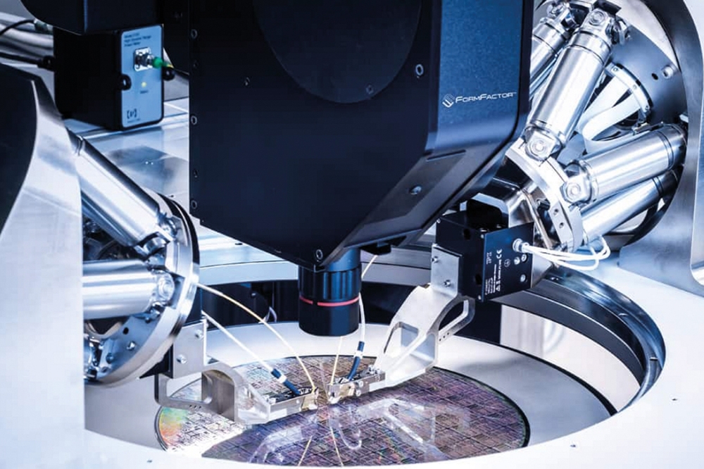
The fabs must allow rapid scalability to meet demand, so yields of circuits such as the ILMZ are critical. We are addressing this through process standardisation, control and monitoring. Batch level automation of processes ensures scalability as well as allowing flexibility and capacity to develop next generation technologies.
Looking forward
We believe that we are now entering a critical phase for optoelectronic semiconductor device development – as more functionality and demands are being pulled back to the chip level, the need to control the chip design, development and timescales is becoming increasingly critical. The industry must grow and make sufficient cash to ensure the next generation of technologies – such as 400 or 1000GbE – can be developed and manufactured at suitable cost. This is driving investment now in basic ‘building block’ technologies and will soon demand further investment in next generation fabrication facilities.
We are starting to ask the questions about how the industry might evolve over the next 5 – 10 years. Will the next generation of photonic fabrication facilities be affordable, even with further industry consolidation? How large will the global requirements for integrated InP optoelectronic circuits become, and how many wafers (3 or 4”) would this require?
If it were possible to set up a complete ‘foundry’ design and fabrication model, would this enable adjacent markets for photonic devices and enable more rapid value growth in the current markets?
To help answer these questions we are working with a number of partners in European (EC) Framework 7 projects such as ‘EuroPIC’. Already external organisations such as Technical University of Eindhoven (TU/E) are designing devices and circuits for fabrication in the Oclaro Caswell facility. There is difficulty here – with the key IP strength moving from process to design.
A key enabling factor will be the establishment of qualified device platforms on which designers can create their circuits. In the silicon microelectronics world, no circuit designer would ever question the design of the underlying transistors and resistors – he or she works at a higher level. Standardization of process allows the fab owner to achieve high volumes and establish a virtuous circle of improvement in process capability and production yields.
Furthermore, by establishing qualification at the platform level (‘capability’ qualification), the designer will be relieved of a major burden in the product development cycle inqualification and reliability proving at the level of individual designs. This way of working is routine in the silicon microelectronics world but in photonics it is new. It will need new ways of working on the part of designers and fabs – and could stimulate new opportunities for fabless design houses and manufacturing companies. It will also require greatly enhanced computer aided design capabilities to support circuit-level optical design.
However this may evolve, we believe that ownership of fabrication facilities and processes right now gives the best possible platform for growth and differentiation in the industry, as well the opportunity to rapidly scale as the insatiable demand for data transmission continues.
![]()


