Infinera touts 'Kish's law' for photonic circuits
The term "Kish s law" could one day be lauded much like Gordon Moore s seminal vision of silicon semiconductor development, following the introduction of a photonics roadmap by California s Infinera.
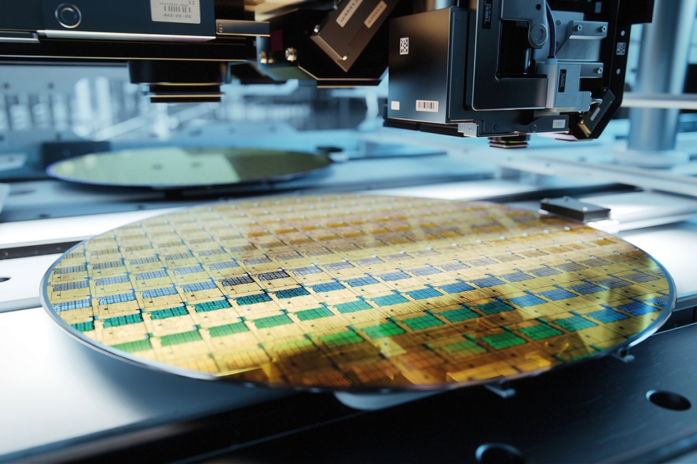
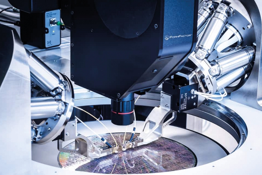
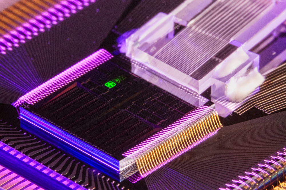
The company, which manufactures InP-based photonic integrated circuits (PICs) that condense huge amounts of optical functionality onto a single semiconductor chip, launched the roadmap to coincide with this week s Optical Fiber Communication (OFC) conference in San Diego.
Fred Kish, the firm s VP of PIC development and manufacturing, and formerly an innovative force in high-brightness LED research at Hewlett-Packard, is the key architect of the roadmap.
Imitating the International Technology Roadmap for Semiconductors (ITRS), Kish s vision anticipates that the capacity of PIC chips will double every three years for the next ten years.
The firm s current PIC, introduced in 2004, offers ten wavelength channels, each operating at 10 Gb/s to give an overall capacity of 100 Gb/s.
The next step is 400 Gb/s, a capacity that Infinera is demonstrating (in a 10 x 40 Gb/s channel form) at this year s OFC, and which it plans to launch commercially in 2009.
Infinera inside?
Unlike the ITRS, the photonics roadmap is not a document ground out of extensive collaboration between myriad chip makers, materials suppliers and equipment vendors.
Rather, it is unique to Infinera, which is positioning itself as the Intel of the photonics world and aiming to commercialize PICs with a capacity of 1 Tb/s in 2012 and 4 Tb/s per chip in 2018.
According to VP of technical marketing Serge Melle, it is not so much the overall data rate that matters, but the density of components on each chip - conceptually similar to the way that semiconductor makers have squeezed more and more transistors onto silicon chips via scaling with lithography.
However, the much greater complexity of photonic components means that the company s 400 Gb/s chip is slightly larger than the current generation.
Merely getting from 10 Gb/s to 40 Gb/s channels has already been a tough challenge, Melle said. The jump in speed demands the use of differential quadrature phase-shift keying (DQPSK for short) to handle the faster modulation frequency. Usually this would be done with a number of discrete optical components, but in a PIC this is not an option.
"40G requires things like splitters, receivers and so on," said Melle. "The component count is huge."
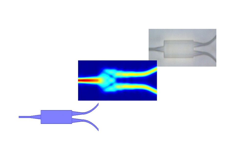
Kish and his team has managed to consolidate all of the required optical functions on the same PIC, complete with all of the necessary active components like lasers, photodetectors, and arrays of Mach-Zehnder modulators.
What s new in the 40 Gb/s channels is that semiconductor optical amplifiers (SOAs) now feature inside the PIC (see related story). And, because they operate over a much wider wavelength span than conventional erbium-doped amplifiers, these devices could provide the key to future increases in chip capacity.
Erbium-doped fiber amplifiers only operate in the 1530-1560 nm wavelength range. In contrast, says Melle, the SOAs can operate at any wavelength across the fiber window of 1240-1650 nm.
Using the entire fiber window rather than a small portion of it might allow for further multiplexing, with lots more wavelengths available to carry data down optical cables.
Although the roadmap is currently Infinera-specific, Melle believes that it may stimulate the photonics industry towards greater collaboration, in much the same way that the silicon industry.


