CyOptics focused on hybrid designs for "TeraPICs"
by Michael Hatcher
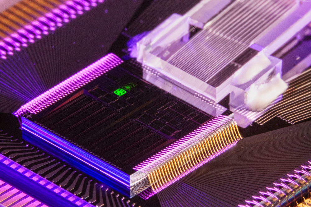
InP optoelectronics specialist CyOptics and silicon photonics pioneer Kotura are working on a $12.7 million project to develop photonic circuits known as "TeraPICs" for terabit-scale optical communications.
The two chip firms are working under an advanced technology program (ATP) award from the US National Institute for Standards and Technology (NIST), with ATP providing $6 million for the three-year effort.
Stefan Rochus, TeraPICs' principal investigator and also VP of marketing and business development at CyOptics, says that the ultimate aim of the project is to deliver a 1 Tb/s connection over one single-mode optical fiber.
CyOptics has already made some progress with photonic integrated circuits (PICs), thanks to a previous project supported by the supercomputer builder Cray and the US Defense Advanced Research Projects Agency (DARPA).
Under the Agency's "high productivity computing systems" program, CyOptics began developing 80 Gb/s transmit and receive optical sub-assemblies (TOSAs and ROSAs), and has also done some experiments on integrating InP optoelectronics to a silicon platform "“ a key element of the latest project.
"Without the ATP funding, TeraPICs would probably be delayed by about 2-3 years," Rochus told compoundsemiconductor.net.
A fundamental aim of the TeraPICs effort is to cut down dramatically the number of individual components required for Tb/s communication, thereby reducing the cost of such a platform. Key to this will be CyOptics' highly automated assembly and packaging capability, which should provide for high manufacturing yields and low overall costs.
In terms of the key technical challenges presented by the project aims, Rochus says that some innovation in InP epitaxy will be required to grow monolithic arrays of uncooled electro-absorption modulated lasers (EMLs). These are required to operate over a wide wavelength span of 80 nm, with high output power maintained across all wavelengths.
Integrating these InP components onto silicon waveguides without losing too much power through coupling and insertion losses also presents a serious technical challenge.
Hybrid approach
While PICs are not a new concept - Infinera and lately JDSU both have commercial products based on the technology - the approach taken by CyOptics and Kotura is fundamentally different, Rochus explained:
"Infinera has developed monolithically integrated transmitter and receiver PICs in InP for dense-wavelength division multiplexing (DWDM) applications. These designs are targeted at optical transport applications and longer reach, and require thermo-electric coolers (TECs)."
"TeraPICs, on the other hand, will be for shorter-reach applications of up to 2 km, with the potential for 10 km. They will use coarse-wavelength division multiplexing (CWDM), and don't need TECs."
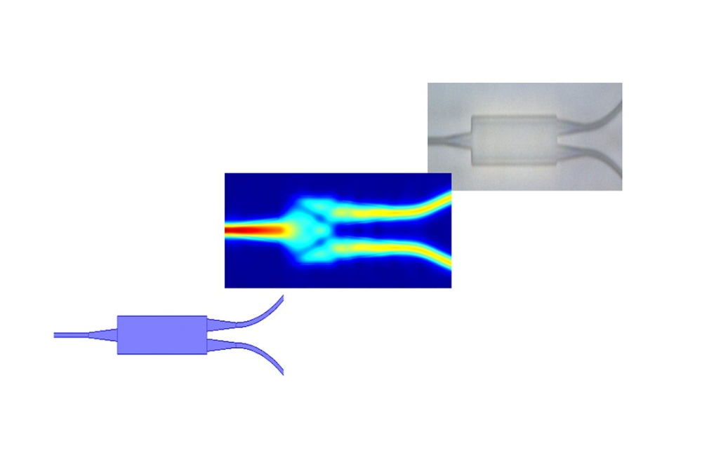
And, while existing PIC technology is based on InP, TeraPICs will use hybrid integration on a silicon assembly platform that will also provide the multiplexing/demultiplexing functions.
If successful, the TeraPICs will be smaller, lower in power consumption and lower in cost than existing technologies, says Rochus.
However, despite the complexities involved in the development, Rochus does not expect any major impact on current InP wafer processing techniques:
"The processes for the lasers and receivers will be the same or very similar to today's processes," he said. "Modifications in the laser designs will address the need to improve the performance of the laser over a wider temperature range (needed for CWDM) and to improve the coupling efficiency from the laser to the silicon chip."
While Rochus does not envisage any major impact on processing, he does suggest that when TeraPICs do become a volume product, there will likely be a need to move to 3 inch or even 4 inch InP wafer processing.
Author
Michael Hatcher is the editor of compoundsemiconductor.net.


