Innovative tricks light up silicon
Don t expect to see commercial, electrically pumped silicon lasers within the next decade. But even if silicon never produces an electrically pumped laser, simple economics indicate that other active and passive optical devices made of silicon are likely to affect the III-V optoelectronics industry. Silicon devices can achieve almost all the necessary functions for integrated optical devices: amplifiers, modulators, switches and detectors. Only an electrically powered silicon light source, preferably a laser, is lacking.
One lure of silicon is the potential to integrate photonic and electronic components on the same chip. Microelectronics companies want to use optics, rather than copper, to ferry more and more data at increasing speeds in shrinking packages. Eventually, light could provide chip-to-chip or even on-chip communications. Silicon also offers the potential to make photonics incredibly cheaply. Alex Dickinson, president of silicon photonics company Luxtera, calls it "the irresistible economics of CMOS". A high-volume silicon chip made via standard CMOS fabrication costs less than chips made from a more-expensive material using less-optimized and less-standardized processes.
Silicon offers technical benefits too. Bahram Jalali at the University of California, Los Angeles (UCLA), explains: "Silicon is the purest and highest quality crystal manufactured by mankind. In addition, it has the highest optical damage threshold of any popular crystal." The large index difference between silicon and SiO2 also provides excellent optical confinement.
The US Defense Advanced Research Projects Agency (DARPA) funds research on CMOS-compatible silicon photonics through the Electronic and Photonic Integrated Circuits (EPIC) program. Its vision statement explicitly guns for III-V devices: "This would enable the integration of complex electronics and photonics circuits on a single silicon chip, eliminating the multiple materials platforms currently used to accomplish such functionality." The EPIC program has funded the work at UCLA, Brown University and Translucent mentioned in this article.
Extracting the lightSilicon is a terrible material for a laser. Lasers usually create a population inversion in which light emission is the most common relaxation path. Silicon, alas, has an indirect bandgap and an overlong spontaneous recombination lifetime. Free-carrier absorption hinders population inversion and Auger recombination reduces light emission. For every 100,000 photons absorbed, silicon emits only one. Inducing it to shed light at all requires invoking nonlinear or quantum effects.
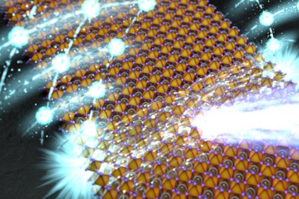
In 2003 Jalali and others at UCLA achieved optical gain in silicon using spontaneous Raman scattering, a nonlinear effect in which light is inelastically scattered by molecular vibrations (figure 1). Raman scattering is a small effect, so one needs a strong pump and low losses to build a laser with this method. In 2004 Jalali s group demonstrated a pulsed Raman laser that emitted at 1675 nm when pumped at 1540 nm. Silicon is opaque through visible wavelengths, but turns transparent in the near infrared.
This Raman laser could only work in pulsed mode because continuous-wave (CW) operation led to a build up of excess charge carriers that impacted the light output. In 2005 researchers at Intel created a CW Raman laser in which the entire length of the waveguide was equipped with a reverse-biased pin diode that swept away the free charge carriers. The lasing threshold depends on the bias voltage in the diode, but this method generates considerable heat (the Intel laser produced 9 mW output power when pumped with 600 mW). In July, Jalali s group reported a method that recovers some of that energy as electricity, thus reducing heating.
Raman lasers are incapable of being electrically pumped, however. Several alternative routes are being explored, explains Sylvain Cloutier at the University of Delaware (Newark, DE), most of which require making silicon act like a direct-bandgap material.
While Cloutier was working in Jimmy Xu s group at Brown University (Providence, RI), they reported creating a silicon laser that works at cryogenic temperatures using sub-bandgap isoelectronic trapping centers. They drilled holes in a thin layer of silicon, pumped this material with a green laser at 514 nm, and extracted weak laser light at 1278 nm. The exact mechanism for the lasing is unknown, but the researchers suspect that the large surface allows a number of silicon-vacancy defects where trapped electrons and free holes recombine. Lasing was observed from 10 to 80 K, but whether the laser can be converted to a room-temperature electrically driven device is another question. The Brown group is also working on manipulating phonons in the material.
Other researchers, such as Lorenzo Pavesi at the University of Trento in Italy, use quantum confinement and the surface-state recombination effects of nanocrystals or porous silicon. Nanocrystals are so small that their electrical structure begins to resemble the discrete energy levels in atoms. The size of a particle dictates the bandgap, and therefore the emission color. Thus, silicon nanocrystals emit light at visible wavelengths.
Nanocrystals have demonstrated electroluminescence with about a relatively excellent 1% efficiency, as well as optical gain. However, short lifetimes have been a problem for these materials. We still do not know what mechanism accounts for luminescence in this material. Pavesi suspects that it is a mixture of two recombination paths in the bulk and at the surface. His group is working on creating an electrically injected silicon laser that emits in the visible by overcoming losses and improving bipolar current injection.
The Trento researchers are also one of the groups combining silicon with erbium or germanium. (Another group is the California-based company Translucent, see "Opaque Translucent"). Pavesi and co-workers are motivated by the potential of replacing erbium-doped fiber amplifiers with a smaller, cheaper, electrically pumped erbium-doped silicon amplifier. In this scheme some of the energy absorbed by the silicon is transferred to the excited state of Er+3 ions, and the erbium releases the light as it relaxes.
Hybrid chipsSilicon might take over all roles except light emission. Luxtera president Alex Dickinson says, "We know that compound semiconductors have a key role." But he adds, "We move a lot of the complexity over to silicon." Luxtera combines optical components with VLSI electronics on silicon chips, betting that the combination of integration and CMOS manufacture will dramatically lower costs. Every component except the flip-chip-bonded laser is made of silicon.
Luxtera sees a market opportunity in the move towards 10 Gbit/s Ethernet. Electrical cabling and power requirements get awkward at this point, but current optical transceivers are too expensive to make economic sense. Lower cost transceivers, especially if they incorporate simple optical connections, could be adopted quickly. Luxtera has intellectual property in a number of key areas, including packaging and modulation. The company is also testing at large volumes: it has made 150 km of silicon waveguides.
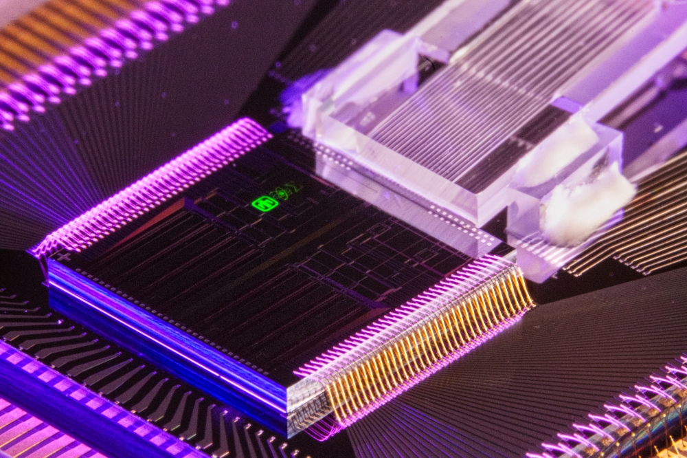
This year Luxtera researchers reported making a CMOS 10 Gbit/s DWDM transceiver chip that contains 50 optical devices and about 100,000 transistors, as well as on-chip lasers. If all goes as planned, the transceiver chips will sell for less than $100. The company will offer sample volumes of transceivers this year, with production quantities available in 2007. These transceiver chips could feature silicon-based ring modulators for switching the light, which Luxtera claims are 25,000 times smaller than Mach-Zhender modulators that are typically made from InP.
Although the efforts at Luxtera show that silicon devices are starting to scratch away at III-V s domain, the impact will likely be small over the next few years. This could however all change if the silicon industry chose to back silicon photonics with multi-billion dollar R&D programs. This funding could improve the performance of many forms of silicon devices, but it is still debatable whether it will ever be possible to make electrically pumped silicon lasers, regardless of how much money is thrown at the problem.
Further readingO Boyraz et al. 2004 Optics Express 12 5269.
S G Cloutier et al. 2006 Advanced Materials 18 841.
http://science.unitn.it/~semicon.
http://www.darpa.mil/mto/epic.
http://www.intel.com/technology/silicon/sp/index.htm.


