Optical integration moves back onto the agenda
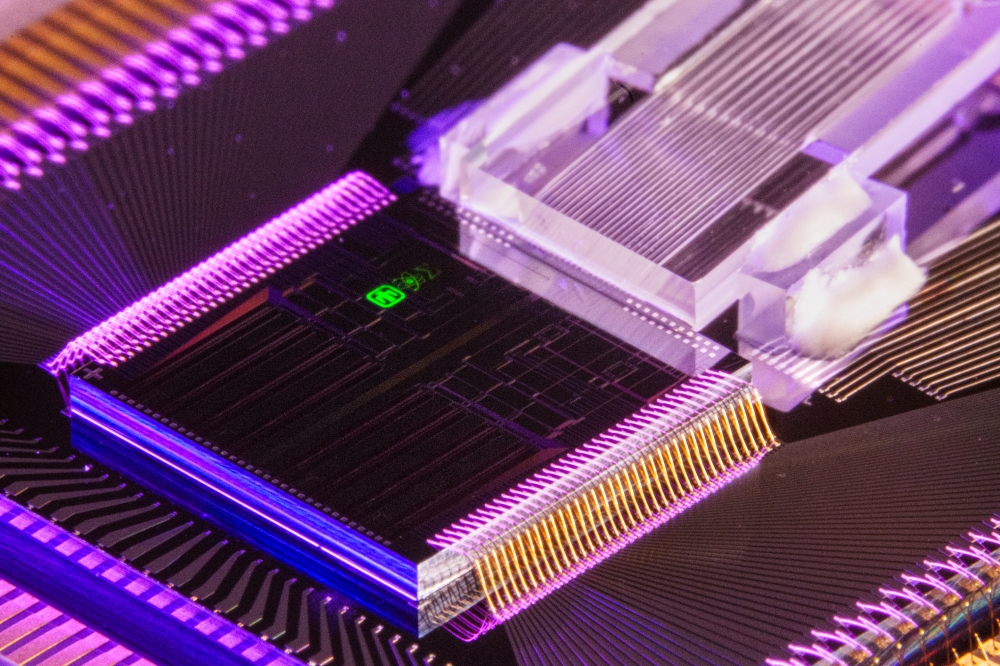
Today, the development of monolithically integrated InP circuits featuring several different optical components is being driven by high-speed transmission, in particular the move towards 40 Gbit/s and the new 100 Gbit/s standards. Indeed, the most widely deployed InP photonic integrated circuit (PIC) to date is an electro-absorption modulated laser (EML) that combines a laser and modulator, while there is also a smaller market for tunable lasers that integrate several functions in a single InP chip. "Tunable lasers are selling in reasonable volumes - several tens of thousands a year - while EMLs are in the hundreds of thousands," says Vladimir Kozlov, founder of transceiver market analyst company Lightcounting.
US firm Apogee Photonics is targeting this market with its 10 Gbit/s lasers. The company has its origins in two InP start-ups: ASIP and ThreeFive Photonics, the latter having brought to market such monolithic devices as a multi-wavelength receiver and an optical performance monitor. Now, Apogee s focus is to exploit its selective-area growth and asymmetric twin-waveguide technologies to optimize the optical functions in its products. "We connect functions using tapers, and with precise control of the composition and structure we can determine the performance of the laser and modulator," says Milind Gokhale, Apogee s CTO.
One example is Apogee s uncooled EML, which operates over a wide temperature range. "It is fair to say that we are using one of the best integration platforms to make more down-to-earth products that the market needs in large quantities," says Erik Pennings, Apogee s director for product marketing.
Pennsylvania-headquartered InP-chip specialist Cyoptics is also making EMLs, as well as tunable lasers under contract for other firms. Like Apogee, its staff have made some exotic PICs in the past. "We made a distributed Bragg grating with phase control, a power detector, and a modulator for a tunable laser over the C-band [1530-1565 nm]," says Robert Hartman, Cyoptics vice-president for device design and development. "We even had a version with a semiconductor optical amplifier that was finished in development." But the market wasn t ready for such devices, he says, and didn t want to pay any more than a 10% premium for single-wavelength (untuned) devices.
Now, however, Cyoptics is seeing renewed interest in PICs. "Regarding photonic integration, some of the meetings I had [at OFC/NFOEC 2006] were the best in five years," says Stefan Rochus, director for marketing and business development, who added that particular interest is being shown in the emerging 100 Gbit/s Ethernet standard.
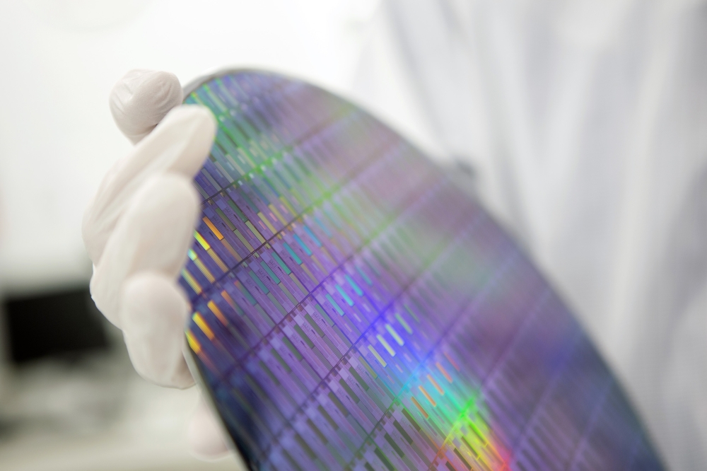
In fact, optical chips operating at these transmission rates are already being built and deployed by Infinera, a US-based vertically-integrated company that manufactures InP chips at its Californian fab and uses them to build systems. The company has even detailed a lab demonstration of a 1.6 Tbit/s optical chip comprising 40 channels operating at 40 Gbit/s. "The reasoning [for such a device] is purely economic," explains Jagdeep Singh, CEO of the US systems vendor. "It is the lowest cost way to deliver bandwidth."
Even though this 1.6 Tbit/s device will not be deployed for several years, it highlights the performance hike that can be achieved. More significantly, Infinera s PIC strategy could signal a forked path in the optical networking industry. Indeed, Infinera s PICs are the optical industry s sole example to date of Moore s Law-style progress.
For now, though, carriers - and by implication system vendors - want to maintain flexibility by using only a fraction of a system s capacity. More channels are lit, or a channel is upgraded from 2.5 to 10 Gbit/s, only when the need arises. "For any WDM system, our philosophy is pay-as-you-grow," says Emmanuel Desurvire, senior director for photonic technologies in Alcatel s photonic-network product group.
When designing a new system, vendors such as Nortel Networks look at the platform specification in terms of the interfaces - and the density of interfaces wanted by the carrier - and the reach. "We look at what new technologies can be brought to bear," says Maurice O Sullivan, manager of physical layer and optical design at Nortel. Depending on the maturity of the integration process, Nortel will consider the technology if it delivers power, size and, in some cases, improvements in system performance.
The cost of integrationAlcatel stresses that adequate trade-offs between different performance criteria must be made when considering integrated products. Adopting an integrated device will probably require the line card to be redesigned, and that adds cost. "The technology also has to be mature and proven - we don t take chances in the field," says Desurvire. "A highly integrated device is not necessarily the best solution. Throwing away what you have can have an impact across the [network] architecture."
With Nortel and Alcatel selling their optical-component divisions, it has also become more complicated to explore how integration can benefit system design. "It is difficult to predict what optical component players are doing and for them to second-guess systems performance," says Michel Belanger, senior technical advisor in Nortel s next-generation optical network group.
Indeed, Infinera s decision to make systems allows the company to put its PIC technology at the heart of its design. "If you don t have control of the optical technology, you can t have a differentiated product," says Dave Welch, Infinera s chief strategy officer.
Infinera s digital transport network (DTN) platform addresses the cost issue of optical-electrical-optical conversions by integrating discrete transponder functionality into its transmit and receive PICs. Infinera will not detail the resulting cost savings, but one carrier suggests that its DTN platform is 30% cheaper than equivalent dense wavelength-division multiplexing (DWDM) systems. Since every wavelength is converted into the electrical domain, whether it is dropped or passed, several other key benefits result. The signal s condition can be monitored, switching and grooming can be performed, and the signal can be properly regenerated - unlike in the optical domain where both signal and noise are only amplified.
Welch claims that Infinera s InP manufacturing process is robust enough to achieve high yield. "We make distributed-feedback lasers in a similar fashion to everyone else, as we do our modulators," he says. What is different is that Infinera gets its engineers to design around the process. "We design what the process can manufacture."
Infinera s design also trades off optics and electronics. Forward-error correction and electronic dispersion-compensation techniques are used to relax the optical specifications, placing more of the link-budget burden on the electronics. Nortel makes a similar point about the importance of integrated components - not just optical, but also analog and digital silicon chips. "Infinera can basically do what others thought impossible because they expanded the domain over which they did their design trade-offs to span systems to processing," says Karen Liu, research director for components at Ovum-RHK.
And while the industry is focused on a pay-as-you-grow approach, Infinera s strategy is to deliver wavelength blocks - in chunks of 10 × 10 Gbit/s - cheaply enough, whether or not they are all needed. Welch argues that a line card costs roughly the same, regardless of what is on it, and the company s PIC shifts the industry from 10 to 100 Gbit/s on a line card. Infinera s prototype 40 × 40 Gbit/s PIC will also deliver a further 10-fold hike in three to four years time.
But Ovum-RHK s vice-president for communications components Daryl Inniss is less optimistic. "A tier-one carrier will not wholly replace its network with Infinera equipment in the next 5 or 10 years," he says. "It s a good idea, a radical idea, but the path they offer is way ahead of incumbent systems."
Baby stepsAs to whether the pace of monolithic integration will hasten in the next five years, most believe not. But that doesn t mean there won t be exciting developments. "Infinera s 10 × 10 Gbit/s is all-in-one-go, but there will be some baby steps by the industry towards its solution," says Inniss.
Perhaps the most exciting is the placing of a tunable laser within an XFP package that supports line-side transmission distances of 80 km and greater. Agility (recently bought by JDSU) has an InP monolithically integrated tunable laser that is sufficiently small to fit within an XFP package.
This development indicates that a variety of transceiver types will converge to one form factor, with one laser and one receiver, says Inniss. Unit volumes will go up, while the price of such a tunable, pluggable DWDM interface will dip below $1000.
Meanwhile, Infinera believes it is only a matter of time before someone breaks away from the pack to make a PIC triplexer. At the same time, advances in hybrid technology continue to reduce packaging costs, and only time will tell which integration method will win.


