Infinera moves in for the long haul as fiber recovers
Californian start-up Infinera has racked up $205 million in venture financing on its way to developing a networking system that is powered by two highly integrated InP chips. Infinera s CTO Dave Welch - who was previously at SDL and then JDS Uniphase, following the pair s high-profile merger in 2000 that was initially valued at $41 billion - describes how Infinera has developed its system using a top-down philosophy and adopting manufacturing techniques used in other areas of the electronics business.
Michael Hatcher: What does Infinera have to show for its $205 million financing?
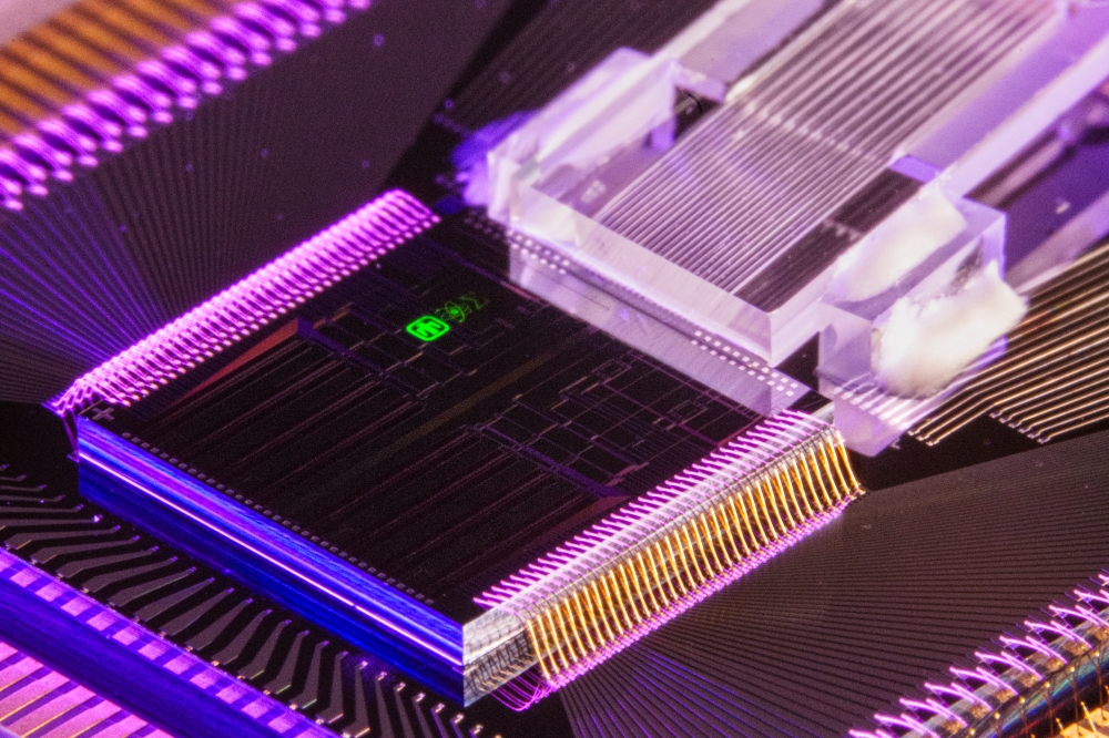
Dave Welch: The majority was there to build a telecommunications system. A smaller fraction was used for the development of photonic integrated circuits [PICs] based on InP. We ve developed two parts, a transmitter and a receiver. The transmitter carries 10 wavelengths, each operating at 10 Gb/s, and combines the functionality of lasers, modulators, electro-absorption modulators and multiplexing elements, as well as structure for wavelength locking and power control.
The receiver side has the inverse of that: the demultiplexer, photodiodes and more control structure. Essentially, we have a standalone 100 Gb/s DWDM transmitter and receiver, based on two chips made here in Sunnyvale at our own facility.
MH: What chipmaking facilities do you have?
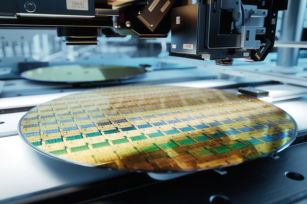
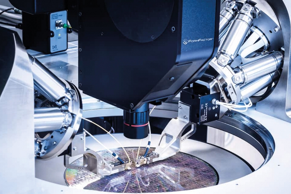
DW: It s probably one of the world s most advanced optoelectronics fabs. We re heavily focused on process control, and have taken a lot of the tools, philosophies and manufacturing processes from the [wider] electronics industry - both silicon and III-Vs - that weren t previously used in optoelectronics, for example our metrology tools. We re also monitoring all of our process parameters, so that we have hundreds of points with which to monitor our process capability.
From a materials and a process control point of view, I can t say we re the absolute best in InP, but we re one of the very few leaders.
MH: How did you go about developing the PIC technology?
DW: We were a bit different to most. First, we set out our vision of the component we wanted to make. We looked at the market and saw that the rest of the world was driving network systems towards all-optical solutions. There are some shortcomings to that approach, and we believed in a different technology.
[For our solution] you need very low-cost optical-electronic-optical components to create a digital optical network. We set out to build a team to make a component that nobody had made successfully before. So we hired some of the best InP design teams in the industry. We also hired guys from the LED industry, because of the very materials-centric, high-volume manufacturing philosophies involved in that business [Fred Kish, Infinera s VP of development and manufacturing, was previously at Agilent Technologies, where he was instrumental in the development of AlInGaP LEDs]. Combining that basic knowledge [of InP] and experience in high-volume optoelectronics manufacturing has been a huge success, and has really enabled us to change the industry.
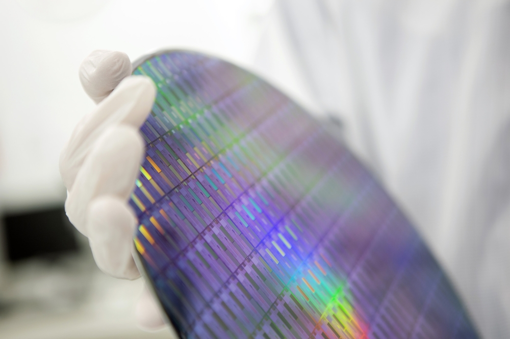
We began shipping products about a year ago and our PICs have been deployed in live networks since last fall. We ve been ramping since then, and are now manufacturing a pretty reasonable number of wafers.
MH: How do you deal with the overheads of running an InP fab?
DW: I don t think the inherent costs of a fab are as great as people state. If you look at distributed feedback [DFB] or Fabry-Perot laser chips, they are cheap and yet come from places where the fabs aren t running 24/7. It is different to silicon fabs - you re using technologies that were built around smaller wafer sizes. We re pushing the technology to the next generation, and so we also run a lot of engineering wafers through our fab.
We ve also developed 10 × 40 Gb/s technology, so we can make a small die with 400 Gb/s capacity. We have engineering projects looking at how to make these things work without cooling, and we ve shown that that s possible as well.
MH: What s driving 400 Gb/s development?
DW: The cost of high-capacity systems is dominated by optics. The more of the optics that you can pull onto a monolithic chip, the greater the impact you can make on the overall cost structure. And if you can get the cost of the transmission components to approach that of the amplifiers then all of a sudden the network architecture changes. Then you ve got a true network where you can add and drop information everywhere in the system, and manage the bits electronically instead of in the optical realm. That gives the carrier a huge advantage through better performance monitoring and bit management.
But the key is to eliminate the cost of converting photons to electrons. If you can make that transformation cost small enough, then you are far better off doing all of the bit management in electronic form.
MH: How can Infinera make the vertically integrated business model work when the likes of Nortel and Lucent have failed?
DW: That s a good question. It s all about enabling the component breakthrough and then taking advantage at the system level. Today, I can t get the components [that I need] for our system from anywhere else and I believe it will be a number of years before such components are commoditized, or are readily available in the outside world. Certainly if they are, we ll focus our fab on areas that give us differentiation.
If you re in the optics business, you need to have control over the optics that give you differentiation. The great breakthroughs in optical communications have been made at the component level. Back in the early 1990s it was the erbium-doped fiber amplifier (EDFA) which changed the landscape in communications systems and enabled the cost benefits of wavelength-division multiplexing (WDM). Nortel rode on the back of two technologies - lithium niobate and III-V materials for 10 Gb/s electronics. Without those component breakthroughs they would have been unable to penetrate the market, as they were not the dominant player in 2.5 Gb/s transmission systems.
On the other hand, we do buy optics from external sources - we use a lot of XFPs on the client side [of the system]. On the line side we feel that we can improve system performance by making something that isn t available in the wider market. But for those companies that are selling what I d call commodity chips, it s a pretty tough market these days. The volumes just aren t there.
MH: How would you describe business at the moment?
DW: Somewhere between very good and exceptional. We re very pleased with the uptake of our product, and when we deploy a 2000 km route, it comes up in a very short amount of time compared to our competitors. That s indicative of the robustness of our product. Customers have been very pleased with that, and at this point the growth rate of our business is exceeding expectations.
MH: Does that growth reflect a general upturn, or are you taking market share?
DW: The majority is from market share - however, the overall market is also growing. All the customers that we ve been engaged with have indicated that data traffic continues to grow at a healthy clip. They ve now exhausted their systems inventories, and their acquisitions of other networks and excess bandwidth have been absorbed. So I think we re starting to see a recovery too. For us, it s a multi-billion-dollar market and we have a chance to take a good chunk of it. We have traffic on our PICs in Asia, North America and Europe, and I feel pretty confident about our prospects.
MH: What are the key challenges facing Infinera now?
DW: Our first phase was very engineering-oriented and company-centric, and we ve rapidly transitioned to being customer-centric. I think a good measure of that can be seen with our Level 3 deployment, which is going really well. Now, the challenge is to drive market share and profit growth while making sure that we re innovating for the next generation.
MH: How do you see the future of the InP photonics sector?
DW: There are some products that will be standardized - I think you ll end up with two or three winners and then half-a-dozen hangers-on. With more modules based on multi-source agreements, only the companies that can differentiate in that area will survive.
It s unclear to me why you need foundries for that type of product. You have to be able to drive enough volume to justify the business that you re in, and by going to a foundry model you just split your profit margin. And there are some foundries out there, so the industry doesn t need to establish them - they already exist. The problem is that there just isn t enough volume in the telecoms market, or the right product set, to do that.
Outside of the component we make ourselves there is a unique set of functionalities [that we require], and if we could find processes capable of doing that then a foundry model makes more sense. However, if all the world wants is lots of DFB laser chips I m not sure that the foundry buys you a lot.
The foundry s value is to apply common processes to lots of different applications, but if there are only a small number of applications then I m not sure about the need for it. If you need a lot of different functions then maybe that model starts making more sense. But, unlike silicon, optoelectronics only has a small set of functions to serve - essentially to transmit or receive light. Until you start trying to manage the bits photonically I m not sure how diverse that set of applications really is.
• Infinera s Fred Kish will present a talk at CS-MAX 2005 on the company s PIC development and the manufacturing methods it has adopted. See compoundsemiconductor.net/csmax for the full conference agenda.


