Intense Photonics Opens III-V Semiconductor Facility For Its Unique Integration-Oriented QWI Process
Provides volume manufacturing for unique integration-oriented process
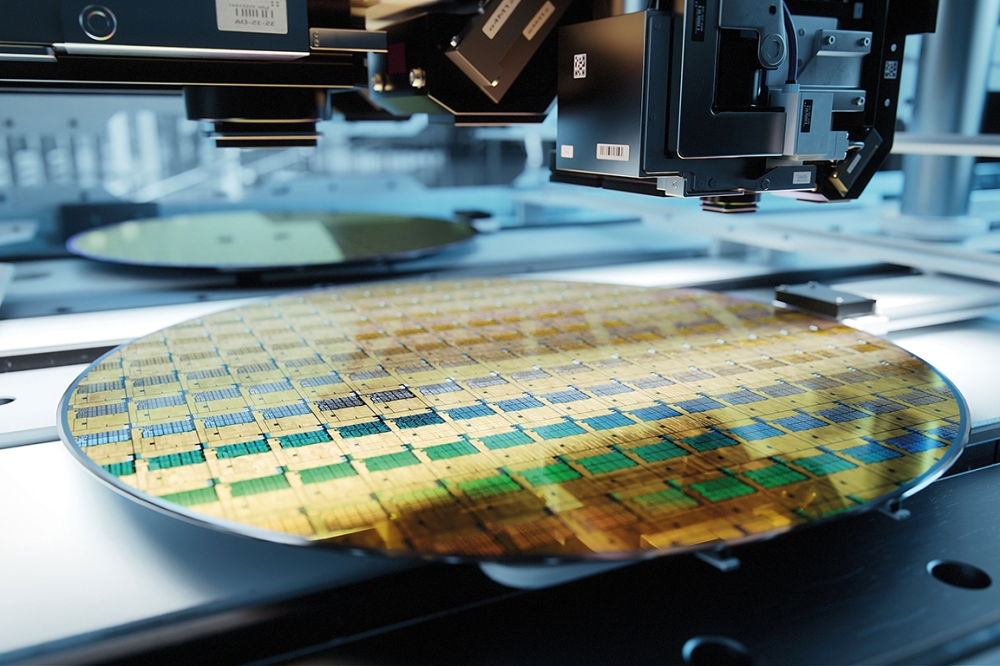
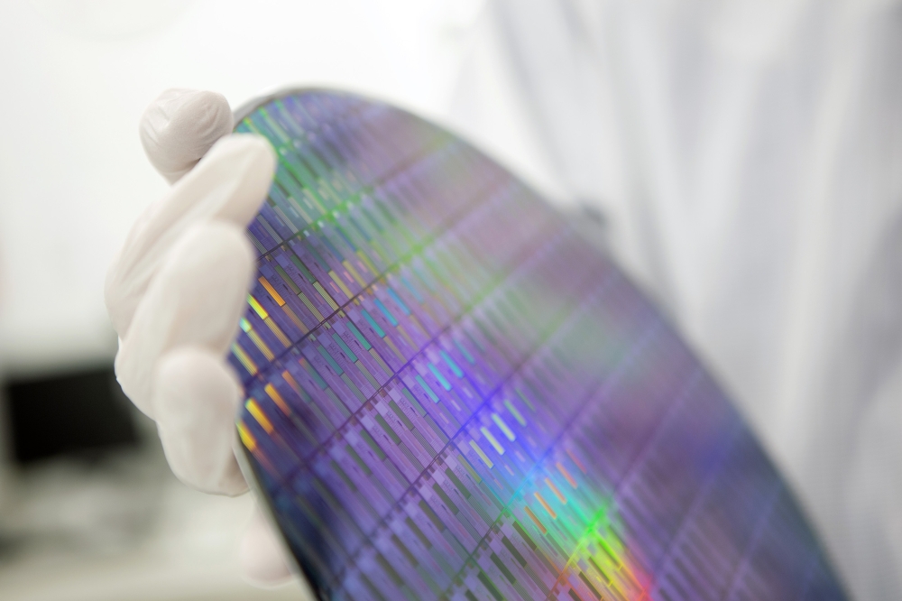
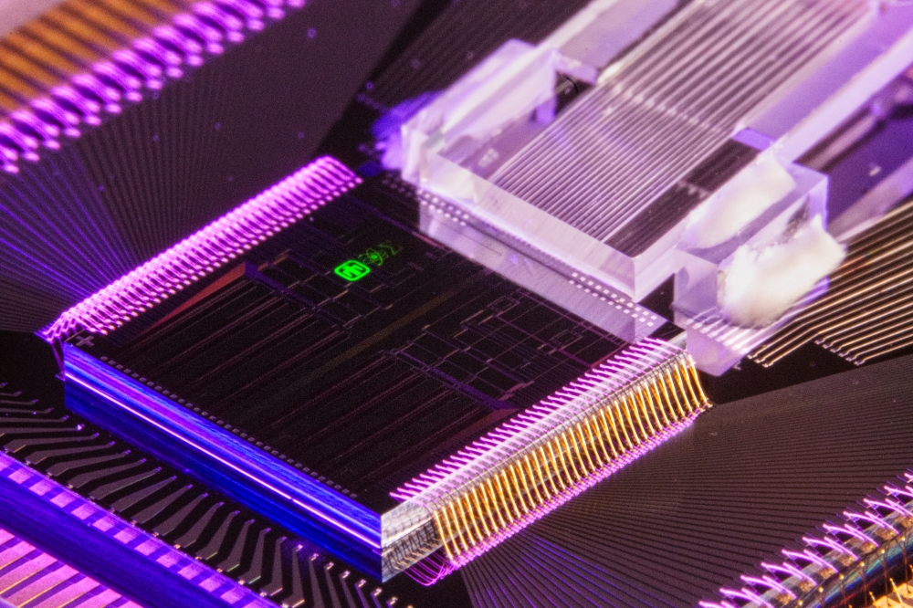
High Blantyre, Scotland. Today, Intense Photonics opens its semiconductor fabrication facility in High Blantyre, Scotland. The specialist facility supports the processing of compound III-V materials for fabricating broadband fibre optic devices, and gives the company complete control over its unique quantum well intermixing (QWI) technology, providing a platform for producing highly integrated photonics ICs.
"Our proprietary QWI photonics fabrication process is at the core of Intense Photonics service. It s a proven way to integrate optical device functions and create more cost effective broadband networking equipment, and this new plant gives us the freedom to begin commercial operations", says David Lockwood, CEO of Intense Photonics. "Despite starting our business during a very difficult period, we ve managed to buy and equip the facility in less than six months, and now have the resources in place to begin working with OEMs to create new generations of optical networking equipment".
The new plant gives Intense Photonics the means to design and prototype optical networking devices, and manufacture them in volume. It can process both gallium arsenide and indium phosphide - semiconductor materials covering all the key optical transmission frequencies in use today and coming into use.
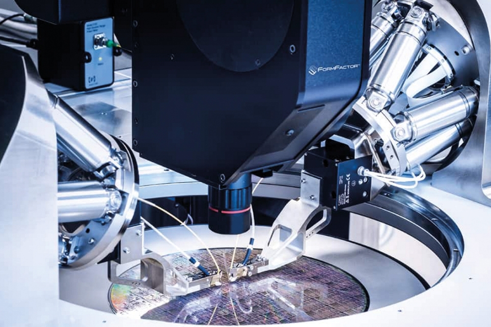
Equipment for designing, prototyping and testing is already in place. The tools for volume manufacturing of commercial products - including plasma-enhanced chemical vapour deposition, plasma and reactive ion etchers, as well as equipment for the company s unique QWI process - will be installed starting in January 2002.
This will allow Intense Photonics to commission the production line and make its first commercial wafer start during the second quarter of 2002. The company will have the ability to make up to several thousand integrated optical devices/month, each integrating multiple functions. The facility will still have capacity in reserve, and expansion room to install further lines in the future.
The company s product plans are based on offering integrated devices combined with customisation services. Its first product is a multi-device array of one of the most basic building blocks of today s optical networks - a 980 nm EDFA pump laser - that may be tailored to suit individual applications. Among the parameters that may be user-specified are output power levels, numbers of lasers on the chip up to 10, physical dimensions and fibre coupling interfaces.
This advance is expected to yield significant savings for system builders. Savings will come from an interconnection design which makes it possible to attach fibre optic cable assemblies easily; from reduced packaging - as only one device must now be temperature controlled instead of up to 10; from higher reliability - because of the dramatic reduction in component count; and from size reductions. Such integration provides the kind of progress that is essential if broadband optical communications services are to move out from the telecommunications network backbone, into metropolitan areas, and finally to the desktop and home.
The company s technology is based on a proprietary quantum well intermixing (QWI) fabrication process which has been trialled over many years on a wide variety of device designs including lasers, amplifiers, filters and switches. QWI allows the properties of a semiconductor material to be modified, typically allowing its energy bandgap to be controlled - making it opaque or transparent to light - such that multiple optical communications functions can be monolithically integrated.
To date, a range of QWI techniques have been developed by industry, including impurity induced, impurity free, implantation induced and laser induced. Intense Photonics process is based on a proprietary impurity free technique, which it believes to be superior as it avoids the optical absorption that results from the introduction of electrically active dopants into a semiconductor waveguide. Intense Photonics impurity free vacancy disordering technique makes use of dielectric caps on the surface of the semiconductor to create vacancies on the group III lattice site. The vacancies diffuse through the semiconductor and, as a result, individual atoms hop from one lattice site to another, intermixing the quantum wells with the adjacent barrier material.
About Intense Photonics
Intense Photonics intends to be a world leading force in the optical communications components market, developing and manufacturing the next-generation of photonic integrated circuits (PICs). It holds the intellectual property rights to optical component design ideas and manufacturing techniques - developed and refined over more than a decade at Glasgow University - that allow multiple optical communication functions to be combined on a single chip. Such monolithic devices are widely viewed as the key to extending the all-optical broadband revolution from the backbone telecom network to the desktop. Intense Photonics technology portfolio includes the semiconductor process known as quantum well intermixing, which allows fibre optic components such as lasers to be monolithically integrated with other functions such as amplifiers, filters and switches - creating a platform to build economic routers and switches for today s DWDM backbones and tomorrow s all-optical networks for metropolitan markets. This proven technology, combined with our strong financial backing, provides the company with a fast route to market. Intense Photonics secured £7.75m first round funding from 3i and ACT Venture Capital in June 2001. It acquired its Hamilton plant - a semiconductor-grade facility built originally for DuPont Photomasks - in July 2001.
What is a quantum well intermixing?
QWI is a technique that allows the properties of a semiconductor material to be modified, typically allowing its energy bandgap to be controlled - making it opaque or transparent to light - such that multiple optical communications functions can be integrated on a monolithic chip. Quantum wells are active elements in opto-electronic (III-V compound) semiconductor devices. Electrons tend to gravitate to the lowest possible energy position and the term wells refers to an area which is [processed] grown especially to have a lower energy, so that it acts as a trap for electrons. They are referred to as quantum wells because these areas are extremely small - of the order of a few atomic layers thick - which makes their operation governed by quantum mechanics, allowing only specific energies and bandgaps.
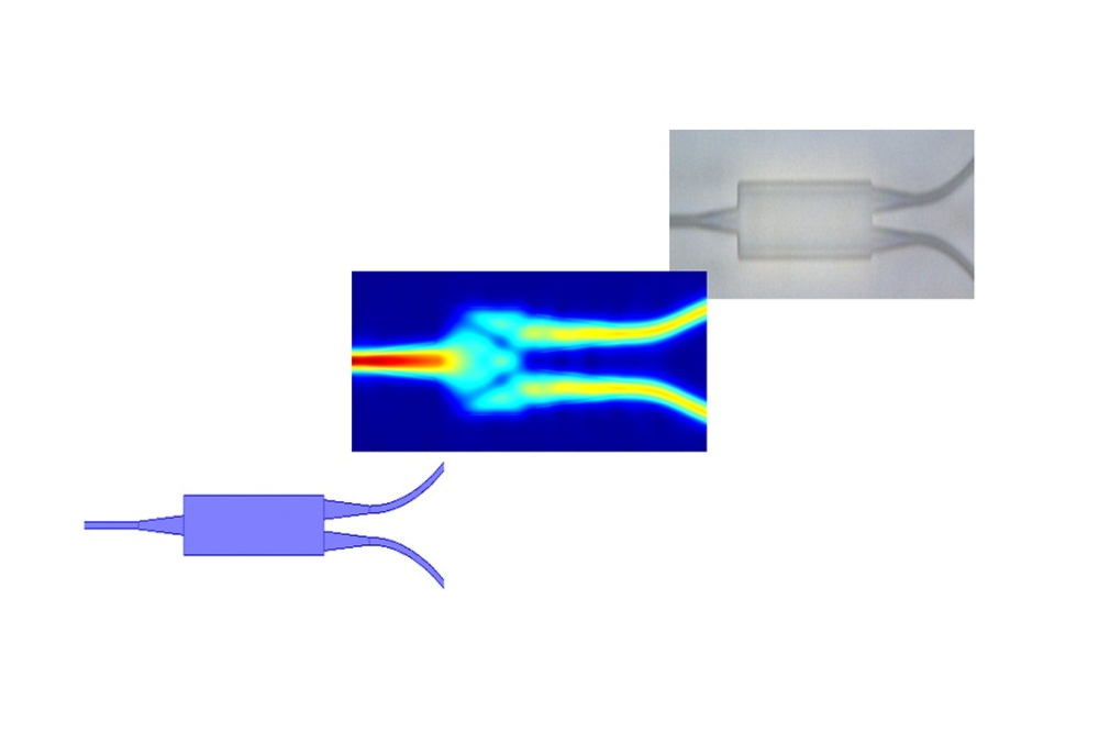
Because quantum well structures are extremely thin they can be affected easily. This is achieved by depositing [or regrowing] additional layers and then applying heat - exciting the atoms and thereby causing intermixing with surrounding materials. By careful choice of capping layers it is possible to selectively intermix the quantum wells across a wafer, thus allowing a single chip to perform various optical functions. For example, Intense Photonics 980 nm pump laser uses quantum well structures to provide more efficient and higher power light output. Quantum well structures improve its performance by forcing electrons from the N material and holes from the P material to be at the same energy levels, thereby optimising the strength of the combination process (which results in photon emission). By closely controlling the thickness of the quantum layer, quantum wells are also used to optimise the wavelength of the emitted light. And, by eliminating the quantum well structures at the device s edges, these regions become passive and transparent to the emitted light, thus preventing a common laser failure mode caused by heating damage. In other devices, QWI principles might be used to achieve absorption - facilitating data modulation for example - or filtering, for selecting and switching particular data transmission wavelengths.
Contact: Intense Photonics Ltd Hamilton International Technology Park High Blantyre G72 0UX Scotland Tel: +44 (0)1698 827000 Fax: +44 (0)1698 827262 enquiries@intensephotonics.com www.intensephotonics.com
Intense Photonics LtdHamilton International Technology Park
High Blantyre
G72 0UX
Scotland
Tel: +44 (0)1698 827000
Fax: +44 (0)1698 827262
enquiries@intensephotonics.com
www.intensephotonics.com
E-mail: enquiries@intensephotonics.com
Web site: http://www.intensephotonics.com


