News Article
BinOptics technology gives more than Moore

The firm's new indium phosphide laser technology helps overcome cost, yield and performance barriers associated with sources for silicon photonics
BinOptics Corporation, a manufacturer and supplier of semiconductor lasers has successfully incorporated its patented Etched Facet Technology (EFT) into a variety of silicon photonic applications.
Creating indium phosphide (InP) based lasers and other photonic components using EFT, opposed to the conventional cleaving process, improves performance, reproducibility, reliability and quality while maintaining affordable manufacturing costs.
Silicon photonics has emerged as a key technology to keep Moore's Law intact for computing in the march towards exaflop (a quintillion or 1018 mathematical operations per second) computing.
Similarly, advances in Datacom infrastructure in recent years have further necessitated cost-effective, highly reliable lasers capable of supporting next-gen high-speed information transfer.
An efficient, reliable, and non-hermetic photonic source is required to provide infrared radiation to silicon photonics circuits.
BinOptics has fabricated semiconductor lasers and other photonic elements on InP that meet these specific requirements.
EFT was first conceived and co-invented by the CEO of BinOptics, Alex Behfar, while pursuing a PhD at Cornell's School of Electrical and Computer Engineering. Since Behfar co-founded BinOptics in 2000, EFT has been utilised in the manufacturing of more than 40 million lasers shipped.
"Our customers have experienced the benefits of our EFT produced lasers for a long time and across a wide variety of applications, but only recently have they been aggressively exploring the unique benefits of our EFT offerings in silicon photonics applications," says Behfar. "EFT is solving a new set of unique challenges as organisations look for solutions to enable the next generation of computing. Many industry experts expect chip-to-chip and on-chip photonics to be the most significant technology impacting the future of computing."
Challenges with reproduction, flexibility, integration, and performance using conventional cleaving processes drive up cost and threaten the sustainability of continuous improvement. The BinOptics EFT design philosophy eliminates those barriers, helping support the rapid advancement of silicon photonics.
Attributes of the technology are listed below.
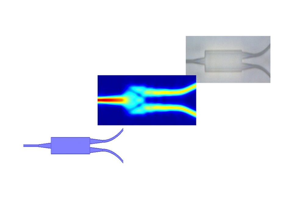
Reproducibility and Flexibility: EFT allows facets to be defined through high precision photolithography rather than imprecise cleaving. The result is unprecedented uniformity and yield, as well as the capability to build structures that are impossible to realise with conventional techniques. With no dependency on the crystallographic plane of the wafer, unique anti-reflection geometries can be used in place of expensive coatings.
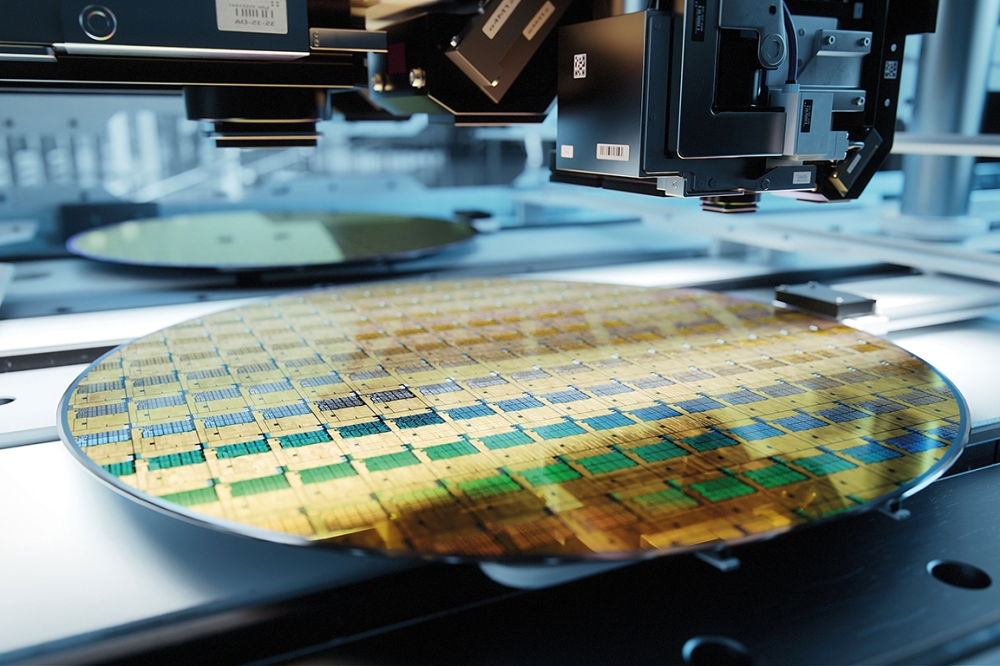
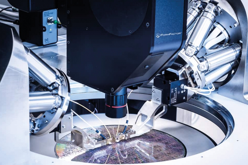
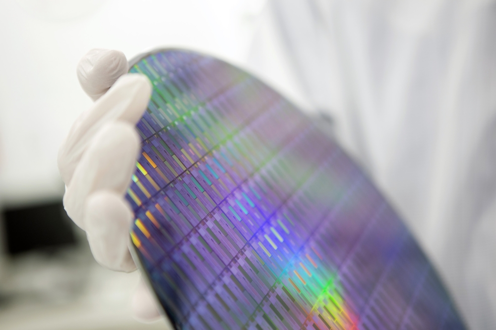
High Yield: Facet cleaving and bar testing is often one of the most costly operations in other factories. BinOptics' lasers are fully fabricated with EFT and automatically tested on the wafer before separation into individual chips. As a result, BinOptics is able to fully evaluate all the lasers on the wafer in an automated, high-throughput test operation, in addition to dramatically reducing the cost of chip handling.
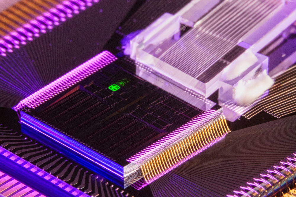
Surface Emission: The BinOptics' technology platform enables etching of angled facets that allow the light from a laser to emerge perpendicular, or at an angle off from perpendicular, to the surface of the InP chip. This is particularly helpful with coupling to grating couplers on silicon photonic chips.
Performance and Reliability: Facet cleaving operation and subsequent coating operations can cause failures and performance issues due to the disruptive nature of the process. EFT eliminates both these sources of failure. Devices made using EFT with proprietary passivation technology are exceptionally robust with respect to temperature and humidity, eliminating the need for costly hermetic packages.
Precision Facet Location: Device facets are formed with extreme precision, enabling low-cost passive alignment with silicon photonics.
"Active alignment of a light source to the silicon photonics chip is a costly process, requiring extremely expensive equipment," comments Jonathan Klamkin, Director of the Integrated Photonics Laboratory at Boston University. "With EFT, BinOptics found a way to reap the cost and efficiency benefits of passive alignment without sacrificing the accuracy associated with real-time active alignment. This should be a critical factor for companies seeking economical, large-scale rollout of silicon photonics applications."
"We needed an experienced but innovative InP partner who could provide a reliable, easy-to-integrate, non-hermetic light source for our silicon photonics platform," concludes Mehdi Asghari, CTO, of Kotura. "BinOptics provided us with the fastest path to market for our new 100 Gbps optical engine, exceeding our expectations in every way."


