Accelerating toward the future of connectivity with photonic integration

The AI-driven surge in data traffic and disaggregated computing demand more integrated optical networking technologies. With expertise spanning photonics, packaging and testing, PICadvanced is uniquely positioned to create customised solutions and accelerate them from design to final product.
By António Teixeira, co-founder and CSTO, PICadvanced
In a world where digital transformation increasingly depends on the speed and efficiency of data movement, the pressure on telecom and datacom infrastructure has never been greater. The shift toward distributed computing systems and the race to support connectivity for growing AI usage demand not only more bandwidth, but also smarter, more integrated photonic solutions, such as co-packaged optics.
At the heart of this transformation is PICadvanced, a company that is redefining how optical systems are conceived, designed, and deployed.
Founded in 2014 and headquartered in the PCI – Creative Science Park in Ílhavo, Portugal, PICadvanced was born from a vision to revolutionise the future of telecommunications with PICs. What began as a bold idea quickly transformed into a reality, driven by a multidisciplinary team of more than 50 engineers dedicated to innovation in photonics, electronics, packaging, and system-level design and integration.
An early turning point in the company’s journey came with the appearance in 2015 of the NG-PON2 standard, a crucial development in the evolution of passive optical networks (PON). NG-PON2 represented a leap in bandwidth capabilities, supporting up to 4 x 10G symmetrical channels. This gave operators more flexibility to enable “pay as you grow”, adding capacity as needed, to offer more services, and to provide a better quality of service for end users. To support this development, PICadvanced specifically created a unique set of end-user transceivers based on advanced components and assembled in traditional sub-mounts. These products combined compact form factors, energy efficiency, and cost-effective performance.

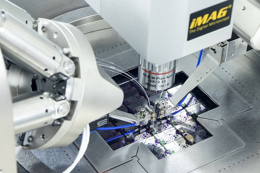
Figure 1. PICadvanced cleanroom view: advanced packaging and testing at scale.
This was where the company’s trajectory took off, but from the start we had our sights set on a broader goal: following the path toward more integrated solutions and building a sustainable future by further minimising footprint, power consumption, and cost. Pursuing this mission, the company has leveraged photonic integration to further reduce the number of discrete components in its transceivers, thus lowering insertion loss.
Another key milestone was the development of PICadvanced’s multi-standard “combo” transceivers, capable of supporting various standards, including GPON (2.5G), XGS-PON (10G), and 50G-PON simultaneously. This versatility allows operators to upgrade more gradually, future-proofing their networks while ensuring co-existence of older and newer technologies to avoid disruptions to service.
These innovations enabled PICadvanced to enter into a competitive market dominated by large-scale transceiver vendors. Rather than compete on scale, PICadvanced differentiates itself through customisation, speed of development, and tight integration between photonics, advanced packaging, electronics, and testing. To this end, the company has been developing the necessary tools to position itself as vertically integrated, conducting the process from design to final product, apart from the PIC fabrication stage itself. In this way, it acts as an accelerator between the fabs and the outsourced semiconductor assembly and test companies (OSATs) at a smaller scale.
Now, drawing on more than a decade of experience, PICadvanced is well positioned to enable the rapid transformation happening in the telecommunications industry today. As carriers deploy fibre deeper into networks and transition toward 50G-PON and beyond, having access to flexible, scalable, and energy-efficient optical transceivers is becoming mission-critical. At the same time, datacentres are moving toward disaggregated infrastructure, such as edge computing, and adopting terabit-scale optical interconnects to keep up with the explosive growth in AI workloads and high-performance computing.
Yet, while these changes are motivated by a need to increase data rates, achieving them requires developments in numerous other aspects of the technology. They demand integrated solutions that can meet stringent requirements not only for transmission speeds, but also for form factor, thermal management, signal fidelity, and cost. This is where PICadvanced stands out, bringing deep photonic design expertise, rapid prototyping, and scalable advanced packaging to meet the complex demands of next-generation infrastructure.

Figure 2. PICadvanced value chain: from optics, electronics and packaging to a product.
Tailored solutions
Dominated by several key players with global supply chains, the optoelectronic transceiver market requires continuous innovation as well as competitive pricing and ever-increasing performance to meet the demands of telecom operators and system vendors. PICadvanced’s approach has been to position itself not as a transceiver manufacturer, but as a design and integration company with deep and advanced photonic capabilities.
By investing in proprietary IP, including photonic chip design, packaging platforms, and thermal management techniques, the company has been delivering flexible, high-performance solutions tailored to specific operator needs. As the underlying foundation of its work, the company has built a platform robust and adaptable enough to solve most of the electro-optic challenges found in today’s high-speed PONs and datacentres.
In an industry where development cycles are critical, the ability to go from concept to prototype gives PICadvanced a distinct edge. Whether adapting a design for a specific optical architecture, or optimising packaging for thermal dissipation in dense environments, the company delivers with agility and flexibility. Unlike many players in the field, PICadvanced does not just assemble components; it builds solutions from the ground up. The company’s fabless yet vertically integrated model enables it to innovate across the value chain depicted in Figure 2.
This positioning allows PICadvanced to offer vertically integrated, rapid-turnaround development and customisation, with a feedback loop between design, fabrication, packaging, and testing. Such an integrated process ensures higher performance, lower cost for smaller productions, and faster time to market – all essential ingredients for competitiveness in both telecom and datacom applications.
Today, PICadvanced employs a team of around 50 highly skilled engineers and scientists, operating in one of the most complete PIC development pipelines in Europe. From design and simulation of photonic structures to full packaging and testing, the company serves as a cornerstone of the hybrid integration ecosystem.

Figure 3. Accelerator and aggregator: photonic-based optical transceiver for access networks.
A key enabler of this integration is PICadvanced’s proprietary silicon-based packaging platform, which allows co-packaging and interoperability of photonic and electronic chips with high-density electrical interconnects, optical interfaces with multiple I/Os, and thermal control and management. The platform is supported by several methods and tools that have been developed in-house, as well as industry-grade equipment, ensuring high-precision die bonding on different platforms and materials, automated and low-loss fibre alignment, and pre- and post-assembly inspection covering 2.5D and 3D die alignment, and optical/electrical performance.
Complementing this is an internal suite of design and simulation tools spanning photonic, electronic, and thermal domains. These tools allow PICadvanced to simulate performance under real-world conditions and optimise across multiple variables – from bandwidth and power consumption to mechanical reliability and signal integrity. Additionally, the company’s facilities also include an ISO7 cleanroom, and assembly and alignment labs with automated optical and electrical testing stations. This equipment provides accurate, high-resolution measurements and advanced packaging capabilities for creating prototypes and pre-series production lines.
Collaborative innovation
While NG-PON2 is now being deployed, PICadvanced is already focused on the next step in the progression of telecommunications networks and datacentres. As the industry moves toward 50G-PON, the company is at the forefront of developing compatible solutions that not only meet the necessary performance standards but go further by supporting combo transceivers – capable of handling multiple PON technologies within the same module. These products offer operators a flexible solution in managing upgrades alongside legacy compatibility, while minimising capital expenditure.
The datacentre space is entering a new era defined by optical switching, high-density interposers, and co-packaged optics. With bandwidth demands doubling every 18 months – fuelled by generative AI and edge workloads – optical integration must evolve in step.
PICadvanced is responding to these needs by contributing to the development of multiple new innovations, including optical interposers for Tbps optical links, advanced hybrid packaging for dense environments, and multi-domain simulations covering photonic, electronic, thermal, and mechanical dynamics. These technologies are being designed to support 200G data rates and beyond for short-reach interconnects, high-throughput switching platforms, and chiplet-based architectures. Through these projects, PICadvanced is becoming not just a supplier, but an innovation partner for hyperscale datacentres and AI infrastructure developers.

Figure 4. Advanced packaging: photonic wire bonding towards a hybrid advanced packaging solution.
With more than 80 percent of its products and services exported to Europe and the US, PICadvanced is already a global player. Last year, the company opened its first international office in the US to support growing partnerships and gain closer proximity to some of the world’s largest telecom and datacentre operators.
In an industry where performance, cost, and time to market often pull in opposite directions, PICadvanced has found a way to merge and optimise all three. The company’s structure, expertise, and vertically integrated capabilities make it uniquely positioned to serve evolving telecom and datacom markets – from chip to product. By continuing to invest in its design, packaging, and integration capabilities – and by aiming for leadership in fast-growing areas – PICadvanced is not only transforming itself, but also helping to shape the broader communications industry and state-of-the-art networking technologies.