Unlocking 3D-CPO: The industry’s first double-sided electro-optical wafer tester

As the telecom industry adopts co-packaged optics at scale, ficonTEC has developed a product strategy that enables volume testing of next-generation optical engines for high-performance computing in datacentres.
By Sung-Hoon Im, Product Management Director for Photonics Test, ficonTEC
Amid the continuing surge in data demands, co-packaged optics (CPO) has emerged as a game-changing solution to overcome the speed and power limitations of incumbent networking technologies.
By moving optical transmission closer to the xPUs, CPO technology contributes significantly to improved operational latency and thermal efficiency compared with traditional chip-to-chip interconnects and high-performance switches. Moreover, this approach simultaneously reduces chip footprint and power demand, making datacentre infrastructure both more sustainable and scalable.
As the telecommunications industry races to make the most of these benefits by adopting more integrated solutions at scale, chip designers together with traditional foundries are increasingly exploring vertically stacked photonic and electronic dies.
Figure 1. An illustration of 3D CPO with vertically stacked optical engines.
Here, diverse second-generation “on-board optics” philosophies are already giving way to next-level CPO.
Central to this shift is the photonic (or optical) engine, a compact CPO module that vertically integrates photonic and electronic components. A prime example is TSMC’s compact universal photonic engine, or COUPE wafer design and reconstituted wafers on PIC substrates, which integrate a PIC with one or more electronic ICs using 3D heterogeneous stacking or polymer overmolding.
The ultimate goal is to bring drivers, transimpedance amplifiers and digital signal processors closer to the optical interface, reducing link distances and power loss across the device (Figure 1).
However, there are many potential pathways to reaching that goal.
In a departure from conventional single-sided chip designs, some innovative architectures require a wafer hybridisation approach that places optical and electrical functionality onto opposite sides of the wafer, yielding a so-called double-sided electro-optical wafer.
Yet as the level of integration increases, novel technologies like these introduce new complexities for the device-evaluation stage; testing both electrical and optical functionality with the required throughput becomes a formidable technical challenge.
For the double-sided wafers in particular, the obligatory test before device singulation requires a test solution capable of characterising optical and electrical performance simultaneously on the opposing sides of a wafer. Until recently, no existing tool had such capabilities. But now, ficonTEC has developed a test system that addresses exactly this need.
Figure 2. ficonTEC’s WLT-D2 double-sided wafer prober (lower right)
integrated with a commercially available ATE. The wafer is located at
the interface between the two systems.
Double-sided wafer testing
ficonTEC is the market leader in high-precision alignment and photonic device assembly automation, celebrating nearly 25 years of designing and manufacturing custom “align-&-attach” as well as “test-&-qualify” production solutions for R&D, new product introduction, and volume manufacturing. Within the last five years, ficonTEC has additionally gained valuable expertise with wafer-level test systems that have been successfully implemented in R&D settings, as well as by PIC development service providers such as VLC Photonics.
More recently, the demand for PIC device hybridisation and device test has been rapidly expanding to include true volume applications. This includes mainstream sectors such as sensors for automotive, for example, but so too in particular for telecommunications applications. For the latter, silicon photonics marks the convergence of PIC applications with established semiconductor technology, both in terms of application and manufacture.
To be adopted at scale in this context, the corresponding optical chip assembly and test production solutions must now be “industry ready”. In other words, they must exhibit top-level reliability and be fully capable within a highly demanding foundry environment. This is a key condition that ficonTEC keeps in mind when designing its test solutions.
By leveraging its own extensive background in sub-micron optical alignment and drawing on the more recent expertise gained in wafer-level test systems, ficonTEC has developed a groundbreaking test system tool designed to enable probing both sides of a wafer simultaneously.
At the heart of this innovation is a newly designed prober platform that enables seamless integration with standard automated test equipment (ATE) as used in the semiconductor industry; while the ATE performs conventional electrical probing on one side of the wafer, the ficonTEC system supports additional, high-precision, multi-channel optical probing on the other (Figure 2).
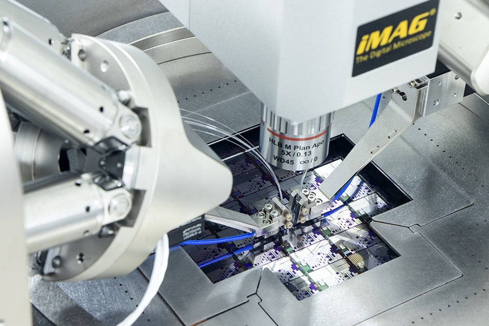
Figure 3. Optical probe aligning to the bottom of the wafer through the slotted chuck.
Designed for the fab
To support high-volume manufacturing and be “foundry capable”, any solution must fully integrate on both a hardware and software level with existing, commercially available ATE setups. ATEs typically operate from the top of a prober for electrical-only testing.
In order to enable simultaneous electro-optical probing with an ATE, the ficonTEC system offers up a custom wafer chuck to the ATE via a 4-axis motion system. This motion system provides the necessary control and precision for positioning the heavy chuck system complete with the sensitive wafer up against the ATE’s fixed electrical probe.
To then successively access each individual device under test (DUT) across the wafer, the wafer chuck assembly is repeatedly traversed.
The system performs optical probing from below via slots in the wafer chuck whose pitch matches the optical I/O placement locations across the wafer. Beneath the chuck, a precision 6-axis alignment module holds a vertically oriented fibre array unit (FAU), which is then positioned to access the corresponding optical I/O location for the current DUT (Figure 3).
During this entire process the ATE remains the master, making the necessary calls to the ficonTEC system to move to the next DUT and to subsequently perform a synchronised electro-optical test, then repeating this process until the entire wafer has been verified.
The system operator must choose the optical coupling configuration – edge or grating couplers – to match the current DUT, and ficonTEC has developed a range of custom FAUs featuring micro-lens tips accordingly (Figure 4). These micro-lenses, fabricated via high-precision 3D printing of organic polymers, refract the beam at the correct angles (usually between 5-23 degrees) while maintaining the alignment accuracy required for optical coupling.
Figure 4. Custom designed multi-channel FAU with 3D printed micro-lens for beam steering and focusing.
A CPO test ecosystem
Beyond its optical and mechanical ingenuity, ficonTEC’s double-sided prober was built for the rigours of high-throughput semiconductor fabs. It supports direct integration with leading ATE systems, ensuring customers can incorporate it while maintaining their existing test infrastructure. Auxiliary features such as probe tip inspection, FAU end-face inspection, automated tip cleaning, optical/electrical calibration, and wafer autoloaders further ensure manufacturing consistency.
Another critical component of wafer-level optical testing, and even semiconductor electrical testing, is cleanliness. Microscopic debris, in particular on an optical I/O, can degrade coupling efficiency, severely compromising the test procedure and ultimately directly impacting effective yield across the wafer.
To address diverse contamination issues, ficonTEC also offers a dry laser spot cleaning module using a 2.8 µm wavelength high-power pulsed laser from Femtum. As the silicon substrate is transparent at this wavelength, only contaminants absorb the laser energy and can therefore be selectively ablated.
ficonTEC’s double-sided fully automated wafer prober marks a major milestone in enabling scalable CPO deployment. Further, it is a critical component of the company’s larger vision to enable the future of a CPO manufacturing and test ecosystem. ficonTEC now offers a suite of test solutions spanning single-sided and double-sided wafer-level testing, as well as singulated die-level testing.
Looking toward the future, the company is currently developing a module-level test platform. Together with ficonTEC’s other solutions, this platform will pave the way for a unified and streamlined test flow, supporting the entire product manufacturing cycle for high-performance optical engines.
As the industry continues its march toward 3D integration and CPO adoption, ficonTEC’s innovations are setting the foundation to enable the high-yield, high-performance computing systems of tomorrow.


