New device co-packages photonics and electronics in scalable design

MIT researchers have reported a new evanescent coupler that increases alignment tolerances and could be manufactured in traditional foundries, paving the way for a cost-effective co-packaging solution and enabling energy-efficient communication
Researchers have reported a new way to co-package photonic chips with their electronic counterparts, which they say solves several problems associated with the current co-packaging process. According to the team, one advantage is that the newly developed co-packaged device can be manufactured using existing equipment in traditional electronics foundries with a less expensive passive alignment process, making it a cost-effective solution.
The future of digital computing and communications will involve both electronics and photonics. Together the two could allow exponentially more data traffic across the globe in a process that is also more energy efficient.
“The bottom line is that integrating photonics with electronics in the same package is the transistor for the 21st century. If we can't figure out how to do that, then we're not going to be able to scale forward,” says Lionel Kimerling, the Thomas Lord Professor of Materials Science and Engineering at MIT and director of the MIT Microphotonics Center.
This is the motivation for FUTUR-IC, a new research team based at MIT and funded by the National Science Foundation’s Convergence Accelerator through a cooperative agreement. “Our goal is to build a microchip industry value chain that is resource-efficient,” says Anu Agarwal, head of FUTUR-IC and a principal research scientist at the Materials Research Laboratory (MRL).
With tens of billions of devices already connected to the cloud, and datacentre traffic scaling rapidly, communication systems consume huge amounts of energy. And “all of it has to happen at a constant cost of energy, because the gross domestic product isn't changing at that rate,” says Kimerling, who is also affiliated with the MRL. The solution is to either produce more energy or make information technology more energy efficient.
Integrating photonics with the electronics that underpin today’s microchips could address the latter because data transmission using light is much more energy efficient. “Our mantra is to use electronics for computation and photonics for communication to bring this energy crisis under control,” says Agarwal.
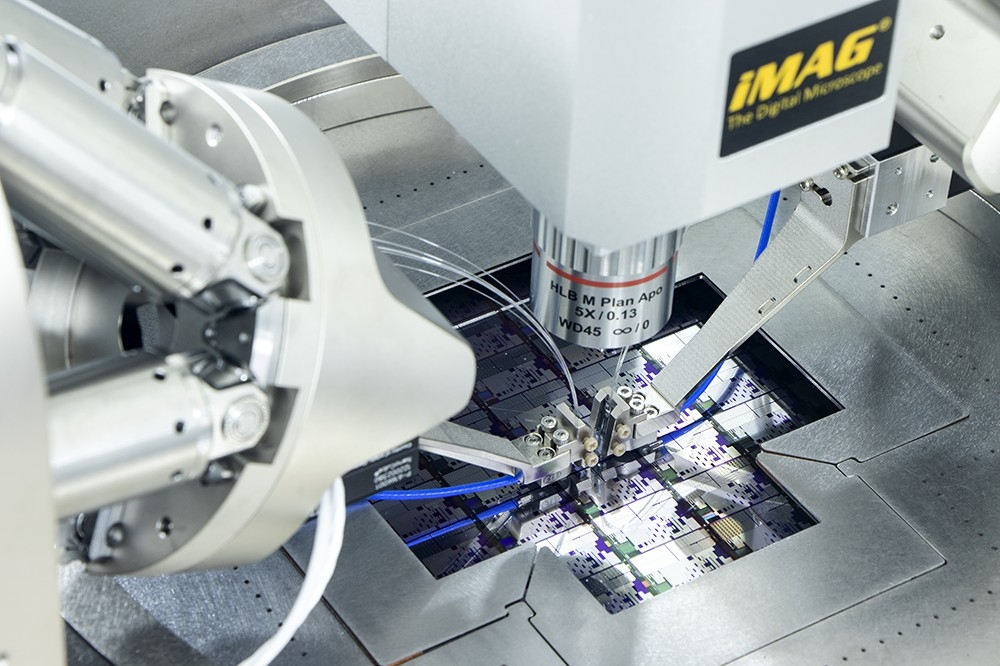
However, this solution comes with its own challenges. For example, it is currently difficult and expensive to connect electronic chips with their photonic counterparts within a single package. That’s because the optical fibre and the photonic chip must be aligned almost perfectly or the light will disperse. As a result, today each connection must be actively tested with a laser to ensure that the light will come through.
“And the number of fibres that we will need for greater data communication is increasing exponentially, so this active alignment process won’t cut it for scaling forward,” says Drew Weninger, lead author on the paper.
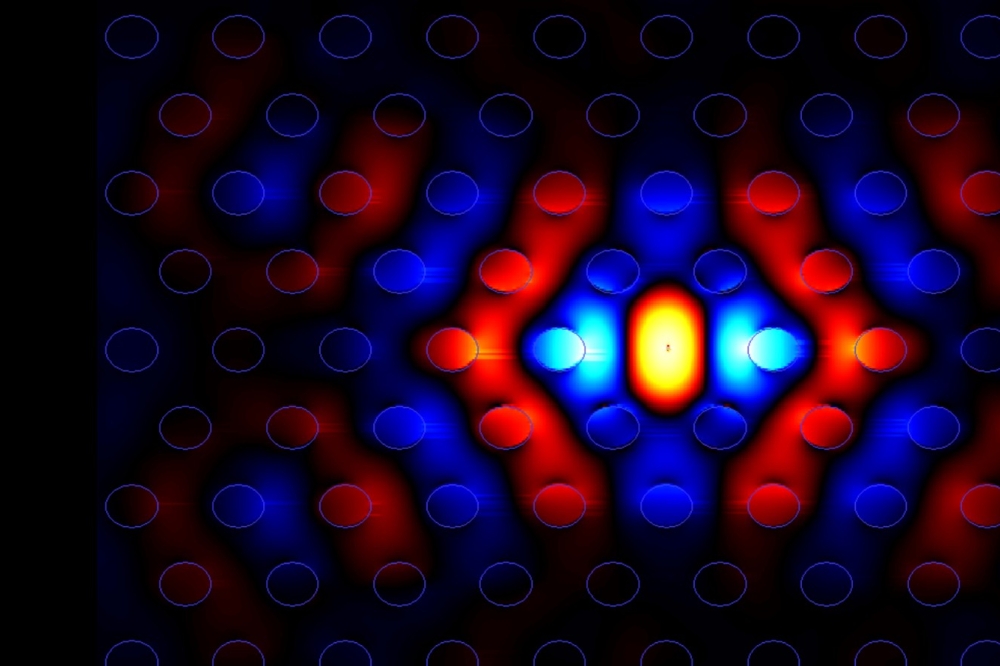
According to the researchers, the new device, called an evanescent coupler, gives much more wiggle room for connecting the fibres within the electronic-photonic package. “Conventional couplers have a single coupling point, making alignment tolerances very tight. But our new coupler has a much larger interaction length increasing the alignment tolerance,” says Agarwal. As a result, robots could passively assemble the resulting integrated circuits allowing more light to pass through without being lost and eliminating the need for active laser alignment, the researchers say.
Additionally, the coupler “allows us to transmit light vertically” between the multiple layers of chips that comprise the whole, says co-author Luigi Ranno. That is itself an important feat, the scientists say, because it is difficult to direct light out of a horizontal plane. “In electronics it is very simple. Electrons can easily flow out of plane,” Weninger explains. In contrast, “light never wants to take right angles.” The new coupler aims to let light make the jump between stacked chips.
“We’ve developed a packaging design [for integrating photonics with electronics] that is reliable, has a larger alignment tolerance, doesn’t lose much light, and doesn’t waste too much space,” adds Ranno. “Basically, it has all the features you want for an efficient and functional interconnect.”