Achieving precision for photonics with multi-chip bonding

With a focus on upcoming trends in advanced packaging, the new multi-chip bonding platform, MEGA, is the latest example of how ASMPT Semiconductor Solutions is pushing the boundaries of precision and speed in semiconductor manufacturing.
By David Felicetti, Product Marketing Manager, ASMPT
We are currently witnessing a global transformation towards a world where machines autonomously interpret data, learn, and act, enabled by advanced technologies such as AI and the Internet of Things (IoT). This intelligence revolution, unfolding before our eyes, depends crucially on invisible connections between chips, between systems, and between technologies. As the semiconductor industry shifts its focus from simple transistor scaling to sophisticated system integration, ASMPT Semiconductor Solutions’ comprehensive packaging portfolio stands at the centre of this evolution.
From automotive applications to datacentres, and from consumer devices to industrial systems, ASMPT’s forward-looking solutions for advanced packaging and semiconductor assembly make it an enabler of the precise and reliable integration of diverse components into unified systems. These technologies form the foundation for the next generation of intelligent applications – especially in key areas such as AI, smart mobility, and hyperconnectivity.
AI is a good example of how applications are driving developments in chip design; as AI workloads grow increasingly complex, the connections between processing and memory elements are becoming critical bottlenecks.
To address this challenge ASMPT SEMI advanced packaging first-level interconnect solutions leverage technologies including mass reflow bonders, thermo-compression bonders with active oxide removal, and high-performance hybrid bonders that ensure maximum precision and reliability.
These solutions enable the creation of chip-on-wafer-on-substrate (CoWoS) packages that integrate AI logic processors with high-bandwidth memory, creating the high-speed, high-density connections that generative AI systems require. The advanced packaging techniques represent a fundamental shift in how computing systems are designed, moving beyond traditional planar architectures to three-dimensional structures that maximise both performance and efficiency
Besides AI, advanced semiconductor packaging technologies also form the foundation of hyperconnectivity, enabling ultra-fast, reliable, and energy-efficient data transfers across IoT, 5G/6G telecommunications networks, datacentres, and vehicle-to-everything (V2X) communications that define the connected world. In these applications, where speed and bandwidth are key, silicon photonics represents one of the most promising frontiers, using optical pulses instead of electrical signals to transmit data at unprecedented rates. Die-attach solutions for silicon photonics and co-packaged optics enable this revolution by providing the nanometre-precision connections these systems require.

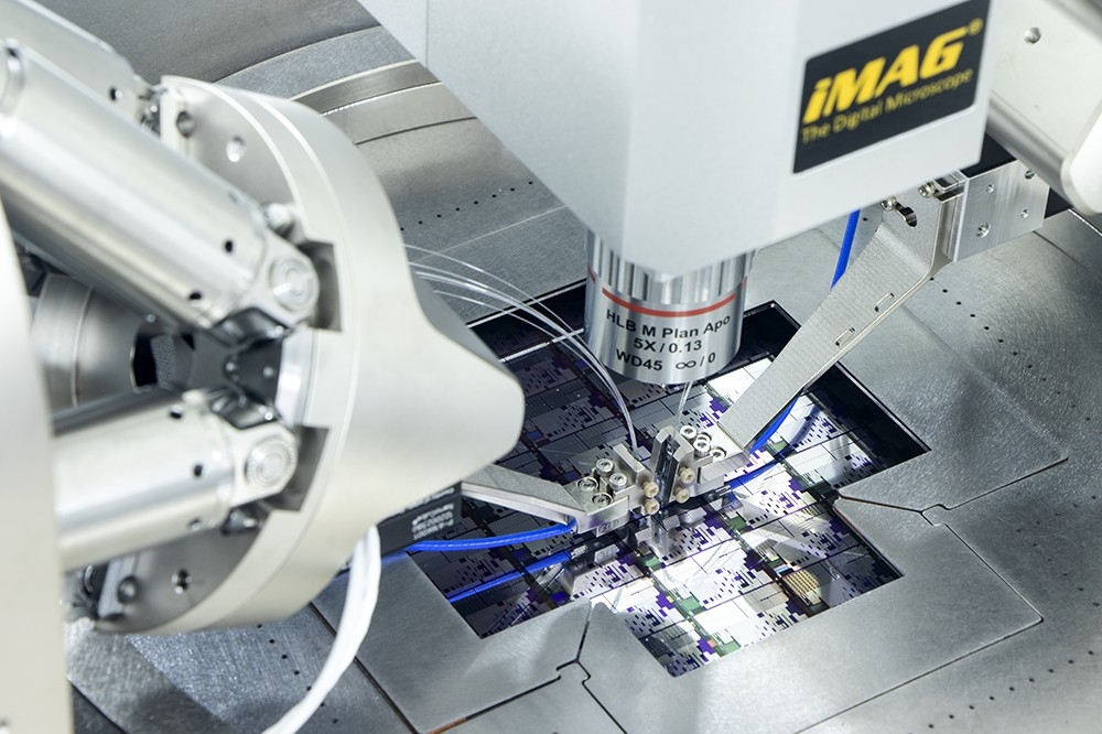
Figure 1.ASMPT’s multi-chip module die-bonder platform, MEGA.
Higher transmission speeds are not the only imperative that is driving advances in packaging technologies for photonics. Take, for example, the development from MEMS LiDAR to flash LiDAR. Whereas the former uses tiny mirrors to mechanically scan a laser beam across its surroundings, the latter illuminates its entire field of view at once with a flash of light and then captures the reflected signals simultaneously with a 2D array of detectors.
Creating flash LiDAR requires the manufacture of arrays of vertical cavity surface-emitting lasers (VCSELs) and single-photon avalanche diodes (SPADs). Both the transmitter array and the receiver silicon photomultiplier made from SPADs put the highest demands on placement accuracy and chip handling. Additionally, this application relies on highly precise alignment of lenses. These stringent requirements for photonics devices are challenging packaging engineers to push their technologies to the next level.
A versatile platform
A wide range of packaging innovations are available to realise high-performance integrated photonics devices, including wafer-level packaging, flip-chip bonding, through-silicon vias (TSVs), 2.5D/3D integration, system-in-package, and fan-out packaging. Machines such as those from ASMPT are available for all of these advanced packaging technologies and the associated work steps, and production lines can be set up to produce the chips.
ASMPT Semiconductor Solutions has set its sights on reducing the high space and energy requirements of such lines by using multi-chip module (MCM) type machines. While ASMPT may not be the only manufacturer with this goal, the MEGA MCM bonder achieves more in many respects than other solutions available to date.
The MEGA chip bonder platform is characterised by high flexibility, a modular design, and minimal space requirements (2550 × 2085 × 1970 mm). Two basic versions are available. The MEGA-G (where G stands for “general”) is designed for maximum speed, processing 12,000 units per hour with an accuracy of ±10 μm at a confidence level of 3σ. The more specialised MEGA-P (where P stands for “photonics”) achieves a reduced speed of 8,000 units per hour, but offers unparalleled precision of ± 2 μm and rotational accuracy of ± 0.1 degrees, both at a confidence level of 3σ. As the name suggests, ASMPT SEMI is targeting photonic manufacturers in particular with the latter device.
Even in the slower, photonics-focused version, MEGA has a higher throughput than competing machines for both die placement and flip chip. With automatic bond tool change, up to 10 bond tool buffers, and five ejector tools, this exceptionally versatile machine adapts quickly to new tasks. The MEGA platform offers various epoxy dispensers and stamp options, the ability to use multiple adhesives in parallel, and automatic switching between application variants.

Figure 2. MEGA’s all-in-one dispense and stamping tool (left) and look-through bond head (right).
For direct application, users can choose between dual dispensing, whereby adhesive deposits are applied line by line at high speed, and highly flexible all-in-one dispensing, whereby any epoxy pattern can be applied, for example for multi-chip applications. In addition, micro-jetting is available for applying low-viscosity epoxy resin, such as that mixed with phosphorus platelets, which is used in LED production.
A special feature is the new 3D inspection of the epoxy application, which measures not only the height, but also the entire profile of the adhesive deposits. This is important, for instance, in high-precision applications where even the smallest changes in process parameters can lead to changes in adhesive behaviour and thus affect the bonding result. Another new feature is the optional instant epoxy stamping unit, which is located directly next to the bond head rather than on the other dispensers. This instant unit provides immediate fixation through UV curing – a major advantage when placing the above-mentioned lenses on optoelectronic multi-chip modules, for example.
Precision and flexibility
The MEGA-P achieves its high accuracy of ± 2 μm with its patented High Precision Bond Head. The look-through bond head allows visual inspection during the process, with pattern-recognition vision systems using the visible edges of the die to determine whether it is being applied correctly. The automatic theta correction and inline quality control ultimately ensure that the machine can achieve a rotational alignment accuracy of ± 0.1 degrees at 3σ. Another detail that increases accuracy is a counterweight that moves back and forth to compensate for vibrations that could otherwise occur due to the rapid movements of the bond head in the machine.
An important design principle of the ASMPT machine is the division of movements and tasks to increase flexibility and shorten distances travelled. The bond track and dispense track move independently of each other, not only in a linear fashion as is usually the case, but also in the x and y directions. The machine can perform dispensing and bonding in parallel without the processes interfering with each other.
This also shortens the distances travelled by the bond head and thus also the travel times.
The decoupling of the chip pickup from the wafer and its placement is highly important too. The picking and bonding arms work independently of each other, allowing space for a flip-pick arm and a rotation unit between them. The rotation unit is used for angle correction and makes a significant contribution to precise alignment. Since even a slight rotation can lead to incorrect positions in the outer areas, this angular correction increases precision, especially for elongated chips.

Figure 3. ASMPT’s look-through bond head is capable of looking at die
edges or at fiducials on the component surface to improve angular and
placement accuracy.
MEGA also demonstrates flexibility in wafer feeding and die and substrate handling. For example, dies can be fed using waffle packs, gel packs, or an optional tape feeder station. The multi-chip bonder processes wafers up to 12 inches and dies from 0.15 × 0.15 mm to 10 × 10 mm, as well as substrates up to 130 × 300 mm.
Moreover, the machine’s customisable options meet the packaging requirements of demanding multi-chip components, making the bonder the first choice for optical transceivers, photonics, sensors, and many other forward-looking applications.
“The MEGA multi-chip bonder performs tasks in a single machine that previously required an entire line of machines,” explains Johann Weinhändler, regional head of ASMPT Semiconductor Solutions Europe and managing director of ASMPT AMICRA in Regensburg, Germany.
“We have made sure that chip manufacturers still retain maximum flexibility. The modular design also allows for customised equipment, so that no one has to buy functions they don’t need.”