Trapping sound waves in silicon photonic chips

Researchers have reported successfully confining sound waves in waveguides on a compact silicon chip, potentially enabling light-sound interactions that could be used to advance wireless communications, quantum technologies, and optical computing
Researchers at the University of Twente have reportedly solved a long-standing problem: trapping optically-generated sound waves in a standard silicon photonic chip. The scientists say their discovery, which has been published as a featured article in the journal APL Photonics, opens new possibilities for radio technology, quantum communication, and optical computing.
Light travels extremely fast, while sound waves move much more slowly. By manipulating the interaction between light and sound – a physical phenomenon known as stimulated Brillouin scattering (SBS) – researchers can find new ways to store and filter information in a compact chip. This is useful in applications such as ultra-fast radio communication and quantum technologies. But doing this in silicon photonic chips has so far been a major challenge.
Silicon photonics is emerging as an important solution to the bandwidth and energy bottlenecks faced by the ever-growing datacentre industry. Introducing sound waves into these chips could unlock an even larger performance boost.
However, conventional silicon photonic structures, known as waveguides, struggle to keep sound waves confined. Sound tends to escape into the silicon oxide layer underneath the silicon structures, reducing efficiency. Previous solutions involved suspending the silicon structures, but this approach introduced manufacturing difficulties, and problems with mechanical stability.
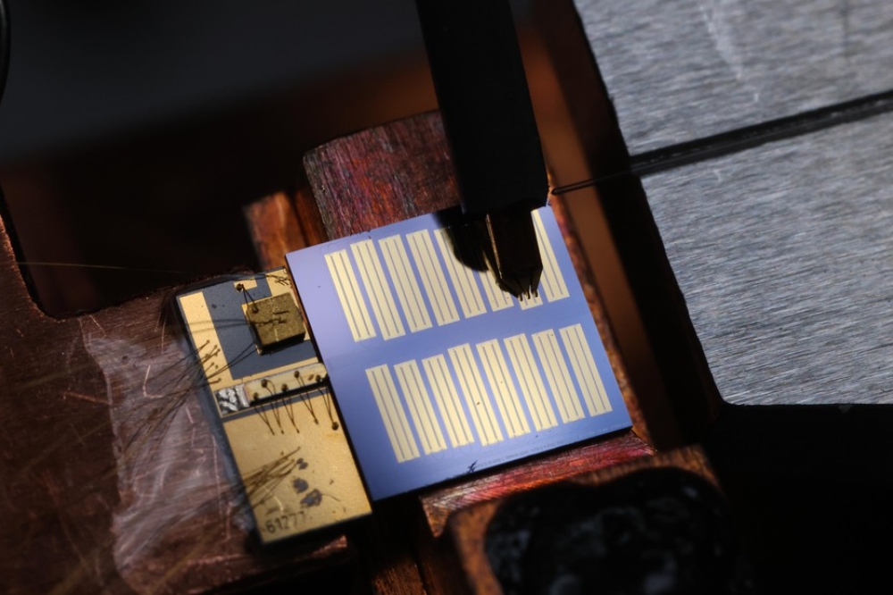
To overcome this issue, the team, led by David Marpaung, took a new approach: increasing the size of the silicon structures. The researchers used waveguides that were 100 times larger than traditional silicon nanowires, and have reported successfully trapping sound waves while maintaining a compact chip design.
“These waveguides from VTT Finland are exactly what we needed to finally trap sound in silicon chips,” said Kaixuan Ye, lead author of the study and PhD student in Marpaung’s group. “Their size makes all the difference, allowing us to control sound waves in a way that simply wasn’t possible before.”
Despite the increased waveguide size, the new silicon photonic chips remain compact and practical, the scientists say, with entire circuits, including metre-long waveguides, fitting within a 1 cm² chip. This makes the technology scalable and compatible with the existing semiconductor industry, ensuring feasibility for large-scale production.
“This achievement took nearly ten years of research and collaboration,” said Marpaung. “By working with VTT Finland and refining our techniques, we finally succeeded in demonstrating this effect in a standard silicon platform.”
According to the researchers, this discovery brings new functionality to silicon photonics, which is already widely used in optical computing and communication. The ability to guide sound waves at ultra-high frequencies of nearly 40 GHz makes this technique promising for next-generation wireless communication and quantum applications.