Tower releases 300 mm silicon photonics process as standard offering

The foundry says that the unique process features best-in-class silicon waveguides and the industry’s most advanced low-loss silicon nitride waveguide offerings, while the larger wafer size enhances compatibility with OSAT platforms
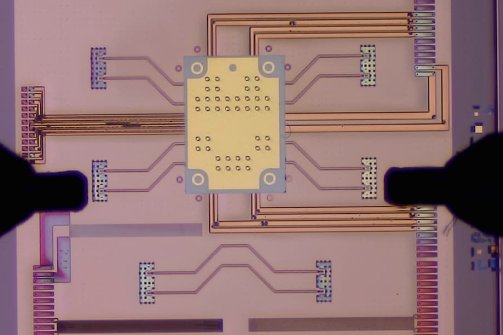
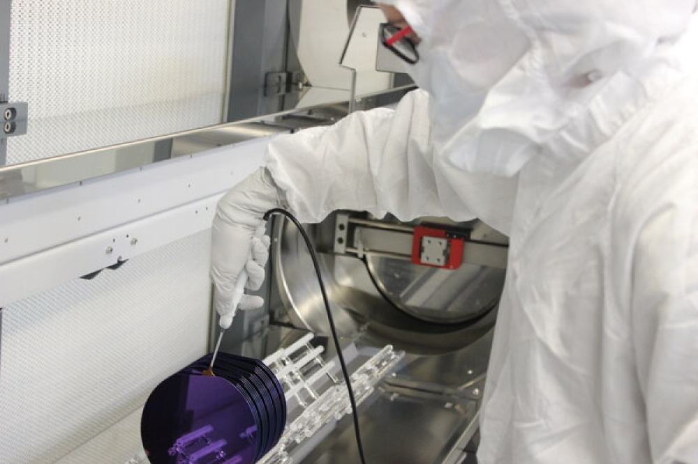
Tower Semiconductor has announced the release of its new 300 mm silicon photonics process as a standard foundry offering. The company says this advanced process complements its well-established 200 mm (PH18) platform that is in high-volume production today, providing its customers with a cutting-edge solution tailored to meet the growing needs of high-speed data communications for next-generation datacom applications.
According to Tower, the unique 300 mm offering features best-in-class silicon waveguides and the most advanced low-loss silicon nitride waveguide offerings in the industry. The larger wafer size enhances compatibility with industry-standard OSAT platforms, facilitating seamless integration with electronic components and improving overall efficiency, the company adds.
“We are proud to introduce our new, highly advanced silicon photonics offering, which provides a seamless path for our existing customers to transition to next-generation technology on 300 mm wafers,” said Edward Preisler, vice president and general manager of RF Business Unit. “This process builds on Tower’s industry-leading 200 mm silicon photonics platform both in terms of continuous process enhancements and increasing flexibility of supply for our customers.”


