Bringing cutting-edge photonics into the classroom

With branches focusing on both industry and education, Spark Photonics is uniquely positioned to bring up-to-date research into its educational programmes, giving school students a glimpse into real-world photonics careers and putting advanced manufacturing on their radar.
An interview with Kevin McComber, CEO of Spark Photonics Design and executive director of Spark Photonics Foundation and Laura Hiscott, Editor of PIC Magazine.
LH: Can you tell me about Spark Photonics and how it got started?
KM: Spark Photonics is a brand name that’s actually two legal entities. There’s Spark Photonics Design, Inc., which is a commercial PIC design services company. Then there’s Spark Photonics Foundation, Inc., which is a nonprofit STEM (science, technology, engineering, and mathematics) educational outreach company. I’m the CEO at the design company and the executive director of the foundation.
The genesis of both entities came from work we were doing at MIT back in 2018 and 2019. I was on staff doing education and workforce development (EWD) as part of AIM Photonics, which is a large PIC initiative out of New York. MIT at the time led all of AIM Photonics’ EWD, and I was assistant director there. When I was hired, it was part of my job description to start up design services. I met my co-founder, Al Kapoor, at one of the AIM events where he was looking for PIC design services. That’s how we came up with the idea for Spark Photonics Design.
At the same time, we felt there was a missed opportunity in K-12 to talk about photonics. AIM was focused mostly on graduate students and the incumbent workforce. We felt that, if we’re going to build a long-term workforce, we’re going to have to start early and work higher up in the funnel of future talent. That’s where we can really move the needle. That was the genesis for Spark Photonics Foundation.
We started the two organisations on the same day in 2019. The foundation found its legs under a US Department of Defense (DoD) grant award to create what is now our flagship K-12 STEM educational outreach programme, SparkAlpha.
We like to think that we’re unique in that the need of the technology side informs the need for the EWD, and that the latter is so closely aligned with industry and led by someone who has a technical background in the subject. We see a lot of EWD organisations led by folks who are traditionally in the education space. Or if they come from industry, they might not be up to date with the current technological advances.
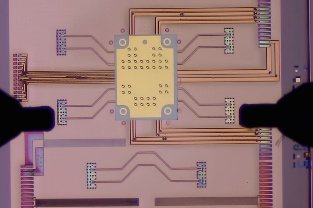
We actively use what we’re learning in design to inform our programming and the material that’s being taught. For instance, we’re working on a project with the University of Rochester and AIM to do sensors for human viruses on a chip, and we use that as an example for students in our educational programmes, because it is happening right now. It doesn’t get any more current than this.
School students participating in SparkAlpha learn about photonics at
Western New England University in Springfield, Massachusetts, an
education partner of Spark Photonics
LH: What role does Spark Photonics play within the broader integrated photonics ecosystem?
KM: For Spark Photonics Design, we were established in large part because the US DoD and the defence industrial base were saying: “We need somebody domestic that can help us design PICs.” Of course, we’ve branched out from defence, but we still have quite a bit of work there. Spark Photonics Design helps companies and others get into PICs from a technical perspective.
We see the foundation as the feeder of future employees into STEM jobs, and to some extent, the very early front door to PICs – as well as more broadly, photonics, semiconductors, and advanced manufacturing. This is how we recruit people into the ecosystem. A lot of us in the photonics industry focus on the tech, but there is no tech without people. We feel, too, that through the foundation, we’re elevating photonics as a branch of STEM at large.
The foundation has a role not only in bringing more people into the PIC ecosystem, but also to use the novelty of photonics to showcase that there is a lot more to STEM than people might think. It’s a unique opportunity to open people’s eyes to worlds they didn’t know about, especially photonics and PICs, and blow their minds.
LH: Could you tell me more about how you work with partners in the industry?
KM: This is mostly on the design side. Spark Photonics Design is the North American representative for Luceda Photonics, a leading PIC design and layout software company based in Belgium. In our partnership with Luceda, we offer a one-stop shop for design services on Luceda’s platform. When our customers become successful and want to take on the design role themselves, we can help them transition onto Luceda’s platform and still support them. It’s a seamless, holistic approach to helping customers be successful in PICs, and it’s possible through this unique partnership.
We’re also OpenLight’s layout partner for customers who want to tape out on their process, which is running at Tower Semiconductor. We use Luceda’s software, and then we use OpenLight’s process design kit (PDK) to help their customers tape out. It increases OpenLight’s capacity so they can focus on their bread and butter, which is the development of that platform.
We don’t have a formal partnership with Ansys, but we use their software to design the components we’ve released at AIM Photonics as part of their PDKs. On our nonprofit side, Ansys has donated to support the growth of our EWD programming. So Ansys has been a very good ally on the foundation side and technology provider on the design side, which is something we would like to see more of – closing the loop between the two entities.
LH: Could you expand on the main activities of Spark Photonics Foundation?
KM: Right now, we have a portfolio of three programmes that are meant to progressively deepen students’ awareness and understanding of photonics, semiconductors, and advanced manufacturing overall. Our flagship programme, SparkAlpha, was created in 2021 and has been running for three years in Massachusetts with almost a thousand students. We’re now expanding nationwide through a US DoD grant employing a “train the teacher” modality. We’re running in Montana and we’re actively seeking more schools across the country to implement this programming.
SparkAlpha is about making students aware of integrated photonics and semiconductors. Through project-based learning, they come up with a problem, address that problem with a photonics hardware product, make a business plan to launch and sell their product at a profit, and then do a live business pitch. They also take two in-person or virtual trips to an education partner – often a college or university – and an industry partner to see what employees’ daily jobs look like.
Next we have SparkBeta coming out this fall. SparkBeta introduces students to the Python programming language, which is what we use on our design side. All advanced manufacturing starts with design, and Python is a very prevalent language that can be used for that. In SparkBeta, students do a mock PIC layout using Google Slides. Then they see an actual layout by one of our design engineers from our commercial side using Luceda’s software, so they can relate to the real-life application.
SparkGamma is the third programme, which we’re planning to roll out in 2025. In this, students learn about how PICs actually work: how light propagates on a chip, some of the basic PIC building blocks, and the process steps to fabricate a semiconductor chip. Then students do an actual chip layout using a PDK with Luceda’s software through a portal hosted by Purdue University’s Chipshub. They create an actual layout file of the chip that could be fabricated.
SparkAlpha is primarily for middle school and early high school, SparkBeta is early to middle high school, and SparkGamma is middle to late high school. SparkGamma is still in development, but we’re getting a lot of good feedback that this three-part progression is something schools would really like to implement.
I also want to highlight that all our staff at the foundation are former educators. They have, on average, over a decade of experience in public education. I’m the only one with a technical photonics background. Although I touted that we have this unique bridge between design and foundation, we’ve consciously strived to make sure that our foundation staff understand education.
They’ve also built up their photonics knowledge. But where the rubber meets the road is getting photonics into K-12 classrooms. That’s best done by people who understand the K-12 landscape, and our staff definitely do. We’ve gone through a lot of iterations to make our programmes really age appropriate. Our staff are also very good at showing schools that this is something that will benefit their students and teachers and the stakeholders at large. They have walked the talk, so they can speak to teachers adopting the programme and explain the benefits.
An employee at Western New England University shows the components of
photonic chips to school students participating in SparkAlpha
LH: Could you describe how the programme is run and delivered in schools?
KM: SparkAlpha was traditionally done with our staff going into the classrooms, typically once a week for six weeks. But of course, that limits scalability when you have to physically be on site. Now, with another DoD grant, we’ve transitioned to a “train the teacher” modality, where we’ve created asynchronous training modules. Teachers can do the training in our online portal, which takes about three hours, and then they’re qualified to run SparkAlpha in their classrooms.
SparkBeta and SparkGamma are self-contained, packaged curricula. They’re meant to be something that the teacher can run without needing to know anything about the topic, and students work through the curriculum and all the activities.
We also add teachers to our community of practice platform, so they can contact other teachers or professionals who are implementing the programme. There are also folks from higher education and industry on the platform, so teachers have this network they can reach out to if they have any questions or need help. This is critical – sometimes programmes like this are just dumped on a teacher, and they are not supported. That’s bad for them and their students. We want to be very thoughtful in making sure they are supported in a way that helps their professional development as well.
LH: Have you had any feedback so far from SparkAlpha participants?
KM: We do a post-programme survey with students, and from hundreds of responses, about 80-85 percent say it’s increased their interest in and understanding of opportunities in STEM. Remember, kids can be harsh in surveys. We’ve got teachers who have seen us run the programme and have now taken on the “train the teacher” modality, because they see the value in it. In other cases, we’ve had teachers take it up without ever having seen it and they have also been successful. I think the fact that we have returning teachers and schools expanding the programme means it’s filling a need.
At the start of every programme when we were running in schools, we always asked the students by show of hands, “Who’s ever heard of photonics?” Usually no hands go up. Maybe one every once in a while. Then we asked, “Who’s heard of integrated photonics?” Absolutely nobody. But then students come out of the SparkAlpha programme having given a presentation to their peers and a panel of judges about integrated photonics. We know that we’re making them aware of the technology and the opportunities in it. We feel that’s moving the needle.
We’ve done some initial teacher testing with SparkBeta. It actually ended up staying pretty similar to how we originally envisioned it. So again, a testament to our staff and their ability to predict how teachers are going to run it.
LH: You mentioned Ansys’ support for the programme earlier. Have other companies in the industry been getting involved too?
KM: Yes they have. Ansys was a donor, but as part of SparkAlpha, students take an in-person or virtual visit to an industry partner. So far our partners have been in Massachusetts because that’s where we’d been running up until the programme launched in Montana. MRSI/Mycronic, MACOM, Convergent Photonics, and IPG Photonics have been partners.
Then we’ve had other folks in the ecosystem who are not necessarily photonics companies but are part of the semiconductor supply chain. We had a company called Innovent Technologies that makes, among other things, the end effectors for the robots that handle the wafers. We’ve had a company called Flexcon that makes plastic sheeting and other plastic components used in the semiconductor supply chain. We try to think broadly about showing students what’s in their community and then making the connection to how that feeds into the semiconductor supply chain. If there’s nothing nearby, especially with rural communities, we can have students do a virtual visit with somebody in the industry and give them time to talk about their career.
When you think about all the components that go into electronic and photonic devices, it’s a very broad supply chain. A large part of the reason for all these CHIPS Act initiatives is that the supply chain is just so expansive and hard to coordinate. We take that as an opportunity to show students that they can be part of the semiconductor industry from a variety of angles.
LH: Last year, you received a three-year grant from the US government to expand your educational programmes. What are your aims for the next two years?
KM: This grant was from the Manufacturing Engineering Education Program (MEEP) of the DoD’s National Defense Education Program. It’s a three-year award, and we’re through year one already. The grant was to create this “train the teacher” modality, which we call SparkAlpha Explore, and then to deploy that first with schools in Massachusetts – that had already run under the SparkAlpha classic model – then to expand within Massachusetts with schools that hadn’t run under the original model, and finally to expand nationally.
We’ve gone from the initial phase of our grant, implementing in schools in Massachusetts that are familiar with us, right to the national expansion, first with Montana. We see a need to demonstrate that it can be successful outside Massachusetts. We need to prove ourselves and have the confidence to say, “Yes, this worked in Massachusetts, and it can also work in Montana, Arizona, California, Colorado, Texas, and more.”
We’re trying to jump toward that national expansion because we see that there are communities that really could benefit from this programming. We want to think big and punch above our weight and get there as soon as we can, because now is the time to do it. We also explicitly want to use our programming to address underserved and underrepresented populations in STEM. We see a huge opportunity in middle school, especially with girls and underrepresented populations in STEM; it’s in middle school that most students are making the choice as to whether they’re going to pursue STEM pathways in high school and beyond.
We’ve gone as young as fifth grade. It’s a very long-term play. For industry and higher education partners, it takes some visionary people to say: “If we’re addressing a fifth grader, they’re probably not going to be part of our student body or workforce for 8-15 years, but that’s where we have to start because that’s where the pool of talent is largest.”
Addressing additional students that otherwise might be intimidated by STEM is something that we very squarely have in our mission. We want more women and underrepresented populations in the industry because we need them.
LH: What are the biggest challenges that you come up against?
KM: After revamping the entire programme, a big challenge is marketing it to people who have never heard of us – and in some cases have never heard of photonics. We found sometimes people feel that what they’re doing is best and there’s a “not-invented-here” mentality. They’re worried about someone else coming in and telling them what to do. However, Montana has a very active photonics cluster, but the mentality was: “Hey, let’s not reinvent the wheel if it works, and we can just plug it in and go with it.” They also said that time is of the essence and we’ve got to get people now. Since SparkAlpha has been proven in Massachusetts, they didn’t see any reason it couldn’t work in Montana. We’re piloting with two teachers in Montana now, and we’ve already had several additional teachers in Montana reaching out to us asking if they could have follow-ons to the piloting. So hats off to Montana.
One big challenge isn’t with the K-12 teachers – who are our ultimate users – but with getting to them, because there are often quite a few gatekeepers along the way. Often the refrain is teachers are too busy and we don’t want to overwhelm them. But we found that there are teachers who are very excited about this and will make the time and the headspace to implement it.
Especially with STEM teachers, they immediately see that this is how they can show students and their guardians that what they’re learning is relevant to their future and relate it to cool things that are happening in the world right now. One teacher told us the hardest question they ever get is: “Why am I learning this?” Now they have an answer.
We find it can be hard to reach those teachers, and sometimes we get screened out. But there are very few people coming to K-12 schools with a proposition like ours. Through our grant, schools are getting free programming in perpetuity related to a society-defining technology that is very much top of mind right now across the world. People generally understand this is something we should bring to our teachers and something we should focus K-12 efforts on, but it is still a struggle for us to get those connections sometimes.
LH: How can people get involved, whether they are teachers, students, or industry professionals?
KM: The crux of this programme is the teachers. We ask teachers to reach out to us through our website or social media, and we will work with them and their administration to evaluate the fit. Students are a great judge of where in their school this could work, but they’re going to need to get us in contact with a teacher or administrator. Administrators know the teachers in their schools or districts who are likely to be very good fits for this.
Industry or higher education institutions can get in touch to be partners for some of the virtual or in-person visits. But at the end of the day, it all comes down to finding the teachers to run it. We are open to teachers broadly – anybody who’s interfacing with students. We can implement SparkAlpha with faculty at two- or four-year institutions. We have run it in community colleges in introductory engineering programmes. It can also be done in summer programmes and after-school programmes, and we’re talking with some folks about running it in museums and libraries. It’s very flexible, but it does need a champion to take and implement it.
That’s our big ask to anyone right now who’s interested in this programme. Help us get to those teachers who will adopt it, and then the sky’s the limit from there.
SparkAlpha participants visit MACOM in Lowell, Massachusetts


