Lightmatter and ASE partner on 3D photonics

The companies plan to combine Lightmatter’s 3D-stacked photonics engine with ASE’s packaging expertise, accelerating the solution to market to offer extremely high bandwidth for scaling AI datacentres
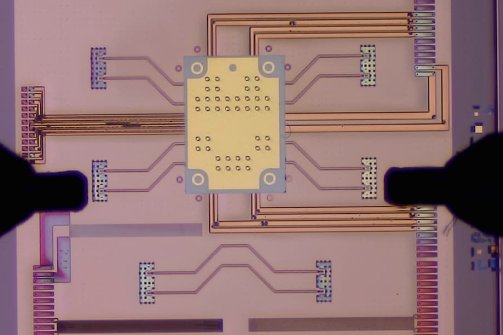
Photonic supercomputing company Lightmatter has announced a strategic collaboration with Advanced Semiconductor Engineering, Inc. (ASE), a semiconductor packaging and testing services provider. The partnership will focus on advancing Lightmatter’s Passage platform, which the company describes as the world’s first 3D-stacked photonics engine with pluggable fibre, to overcome the critical AI interconnect bottlenecks hindering today’s datacentre infrastructure. Lightmatter says this breakthrough enables scaling to millions of XPUs at the speed of light to meet the unprecedented demands of AI workloads.
Scaling compute infrastructure to address the next generation of frontier AI models requires very large numbers of XPUs to be closely connected with extremely high bandwidth and low latency. According to Lightmatter, Passage can directly connect over a thousand XPUs in one domain and deliver from tens to hundreds of Terabits per second of optical connectivity in a single multi-die package. Together, the company says these advances represent an orders-of-magnitude increase over current solutions that utilise pluggable optics.
“ASE’s unmatched expertise in semiconductor packaging and their wide deployment across the industry makes them the perfect partner for us as we expand our Passage platform,” said Ritesh Jain, SVP of Engineering and Operations at Lightmatter. “This collaboration allows us to push the boundaries of silicon photonics packaging, addressing the most pressing needs of high-performance computing and datacentre applications.”
CP Hung, Corporate VP R&D at ASE, added: “We are thrilled to work with Lightmatter to advance their Passage technology. Our collaboration is a terrific example of how ASE’s 3D integration capabilities and large-scale packaging can help bring innovative solutions to market faster, supporting the demand for continued performance scaling in AI silicon.”
Unlike 2D optical chiplet solutions that are limited by the chip shoreline, Lightmatter says its 3D-stacked photonics engine enables I/O to be placed over the entire chip surface area, dramatically increasing the bandwidth and freeing chip shoreline for other needs including memory expansion. By partnering with ASE, the company seeks to deliver a photonics-optimised 3D packaging solution that empowers its customers to massively expand high-speed connectivity to their chips and rapidly scale the production and deployment of the most advanced GenAI superclusters.
The joint effort between Lightmatter and ASE also aims to address the need to directly incorporate pluggable fibre attachment points for all-optical interconnect scaling at very high fibre density in a reliable and serviceable manner. The companies say this innovation represents a significant step forward for the industry in delivering enhanced performance and efficiency for large-scale AI datacentres.


