Lightmatter and Amkor team up on 3D photonics packaging

The companies plan to build the world’s largest 3D photonics package, addressing the needs of AI workloads by boosting bandwidth and reducing power consumption
The photonic supercomputing company Lightmatter has announced a strategic partnership with Amkor Technology, Inc., a provider of semiconductor packaging and test services, to create the largest-ever 3D-packaged chip complex utilising Lightmatter’s Passage platform. This collaboration aims to harness Lightmatter’s 3D-stacked photonic engine along with Amkor’s advanced multi-die packaging expertise to meet the unprecedented interconnect scaling and power demands of today’s AI workloads.
With the end of Moore's Law, scaling AI performance at the chip level increasingly requires integrating more silicon in a single package. Many GPU and accelerator providers address this by incorporating multiple processor, memory and I/O chiplets onto an electrical silicon interposer. While this approach boosts compute capabilities within a package, the I/O bandwidth of the chip is severely constrained by the limited shoreline and the competing need to integrate more memory.
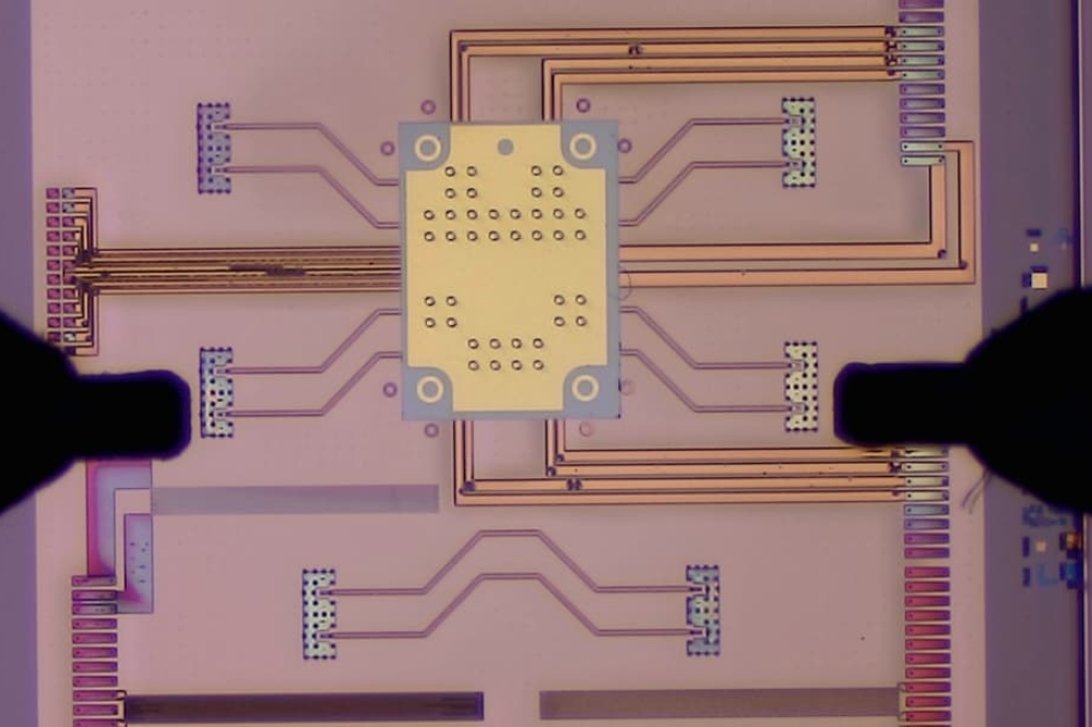
According to Lightmatter, its Passage platform overcomes these shoreline constraints by using 3D integration of customer dies directly onto a silicon photonic interconnect, enabling optical I/O anywhere across the chip area. The company says the platform also provides significantly higher connection density and bandwidth both within and outside the package, and natively integrates optical circuit switching (OCS) within the interconnect, offering enhanced resiliency and flexibility in interconnect topology. Through their partnership, Lightmatter and Amkor aim to deliver unmatched advantages of this combined solution to customers, enabling the industry’s largest multi-reticle die complex on an organic substrate within a 3D package.
“We are delighted to partner with Amkor on a 3D photonics solution that pushes both the boundaries of advanced packaging as well as silicon performance,” said Ritesh Jain, SVP of Engineering and Operations at Lightmatter. “This collaboration is a pivotal step in building a world-class ecosystem that empowers our customers to realise AI and HPC compute offerings with unprecedented bandwidth and efficiency.”
As AI processors grow larger, so does their power consumption, doubling every two years. Lightmatter says that Passage, an all-photonic silicon interconnect layer, addresses this challenge by seamlessly integrating into a 3D package, enabling superior energy efficiency and performance, particularly in demanding thermal conditions. The company says that its combined expertise with Amkor in photonics and 3D packaging has led to a breakthrough that unlocks unprecedented silicon density and bandwidth within a single package, paving the way for the next major computing advances, including AGI.
“As a leader in advanced semiconductor packaging, we are thrilled to collaborate with Lightmatter on integration with their cutting-edge Passage platform,” said Kevin Engel, EVP, Business Units at Amkor. “Leveraging our deep semiconductor integration expertise, we are working closely with Lightmatter to develop and validate a robust 3D packaging solution to bring this groundbreaking silicon photonics technology to mainstream market availability.”


