OKI develops ultracompact PIC for optical sensors

The company plans to capitalise on the advantages of silicon photonics technology to develop various optical sensors that can be applied to social infrastructure and contribute to green transformation initiatives
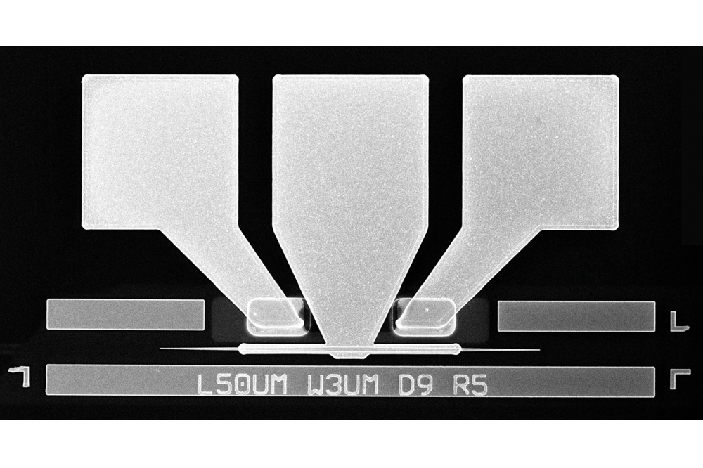
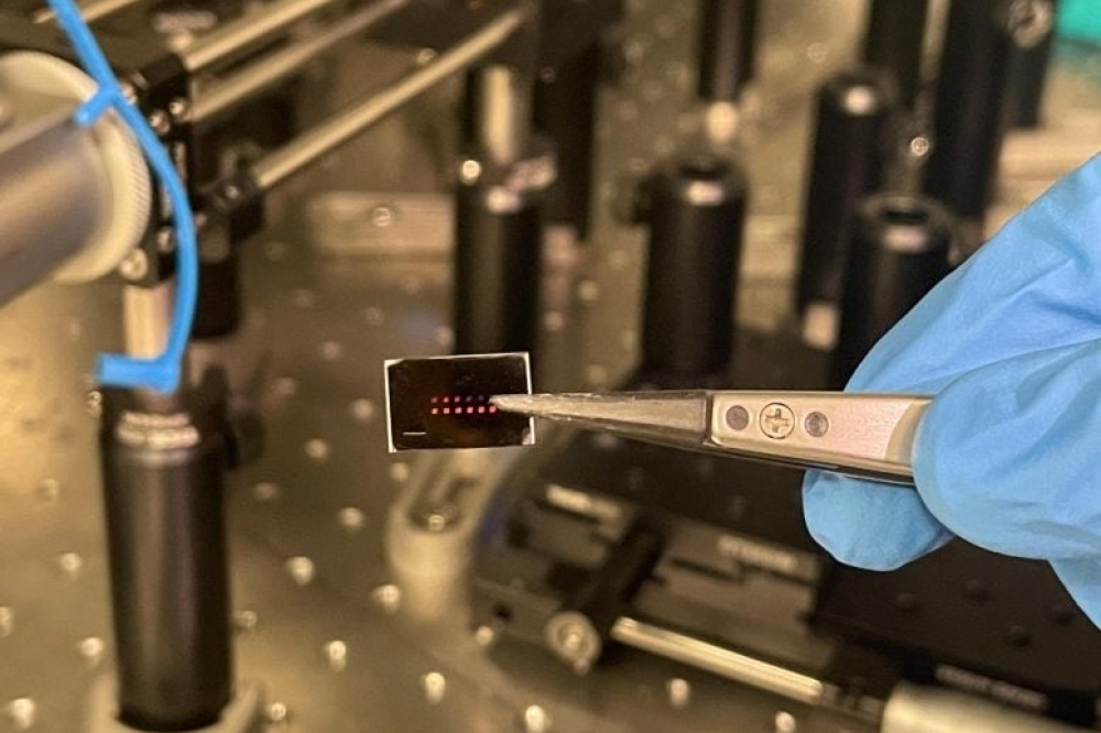
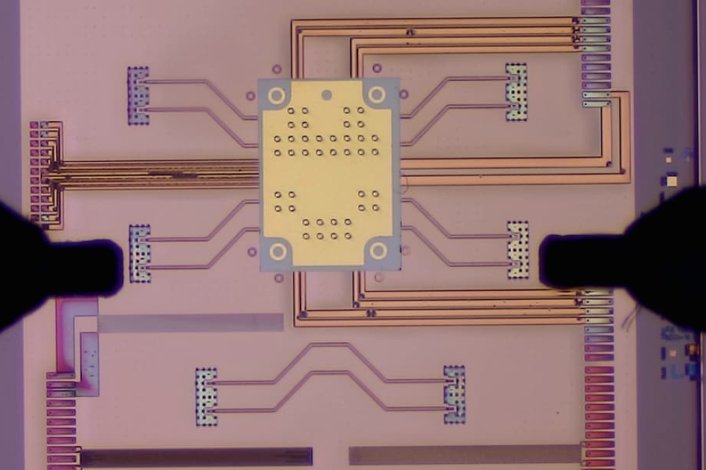
OKI, a Japan-based information and telecommunication company, has announced that it has used silicon photonics technology to successfully develop an ultracompact PIC chip with a broad range of potential applications, including optical fibre sensors, laser vibrometers, and optical biosensors. The company says this makes it possible to achieve ultra-miniaturisation and low power consumption similar to large-scale integration (LSI), as well as dramatically lower costs through mass production of optical sensor modules.
Optical sensors are a technology that uses optical fibres and optical waveguides with low light loss to detect, process, and transmit physical phenomena such as vibration, strain, and temperature in the form of light, and are themselves a green technology that realises sensing while saving energy. Silicon photonics technology can broaden the scope of applications for optical sensors previously limited to localised use, and is expected to make a significant contribution to the advancement of green transformation initiatives.
To address various issues faced by modern society, such as aging social infrastructure, labour shortages, environmental problems, and extending healthy lifespans, high-precision sensor technology and network technology capable of seamlessly collecting vast amounts of sensor data are required. While high-precision optical sensors that take advantage of the property of light, i.e., low energy loss, are one effective technology to realise the above, their large size and high cost have limited their applications to a few areas such as research and large-scale infrastructures.
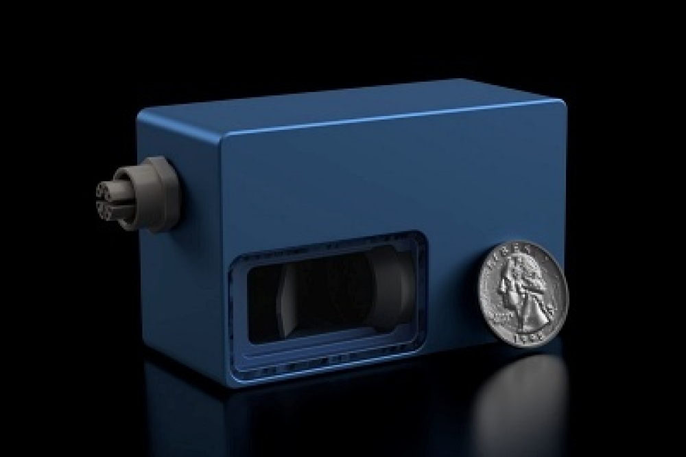
OKI says it has engaged in R&D on silicon photonics technology over many years, centred on optical transceivers, with the scope of this research still currently expanding to include various optical sensors. Silicon photonics integrates complex optical circuits – previously realised by wiring individual optical components with optical fibres – on a silicon substrate using semiconductor microfabrication technology. It makes use of the same manufacturing methods as LSI, which is vital for computers, enabling miniaturisation, energy saving, and cost reduction through mass production. Devices that were previously large, heavy, and cumbersome can now be downsized to dimensions comparable to a smartphone or tablet, greatly expanding the scope of optical sensor applications.
In November 2023, OKI announced its technology strategy through to 2031, which is aimed at bringing the Edge Platform to reality. The Edge Platform is a technology concept to expand the value provided through edge advancement and data connection and linkage based on OKI’s core competence of “robustness,” which has supported social infrastructures. The technology strategy includes bolstering optical sensing technology across a wide range of areas, from social infrastructure monitoring to the medical field. The development of this PIC chip is based on this technology strategy and is the result of fully capitalising on silicon photonics technology.
“Based on silicon photonics technology, OKI will continue to scale up PICs incorporating semiconductor materials other than silicon as light sources and promote photonics-electronics convergence to expand into ever more diverse fields,” commented executive officer Kurato Maeno, who also serves as chief technology officer and head of Technology Division. “Ultimately, OKI aims to realise a universal integrated circuit chip that enables the programmable implementation of various functions on a single chip and make the most of this as the core of its green technology.”


