New ultraprecise technique for aligning 3D stacked chips

Researchers say that their new method, which uses lasers and holograms, can detect misalignments down to 0.017 nm, and could be used in the production of 3D photonic and electronic chips
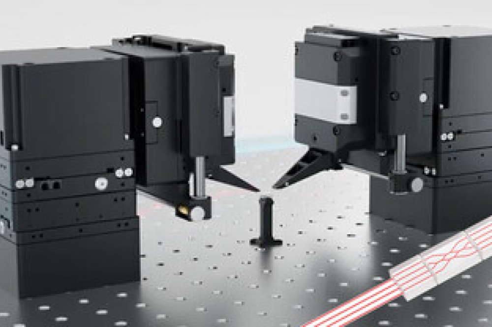
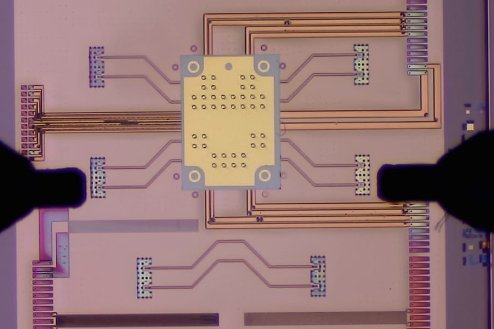
Researchers at the University of Massachusetts Amherst have invented a new way to align 3D semiconductor chips by shining a laser through concentric metalenses patterned on the chips to produce a hologram. The team says their work, published in Nature Communications, can help to lower the cost of producing 2D semiconductor chips, enable 3D photonic and electronic chips, and may pave the way for other low-cost, compact sensors.
Semiconductor chips enable electronic devices to process, store and receive information. These functions are controlled by the specific pattern of components inlaid into the chip. However, this 2D design has reached its upper limit of technological advancement and 3D integration is considered the most promising solution.
To make a 3D chip, multiple 2D chips are stacked and their layers need to be aligned down to tens of nanometres. Furthermore, they need to be aligned along three dimensions — forward and back, left to right, and the gap between the two chips (along the x, y and z axes).
“The traditional approach for aligning two layers is to look with a microscope for marks (typically corners or crosshairs) on the two layers and to try to overlap them,” explains Amir Arbabi, associate professor of electrical and computer engineering at UMass Amherst and senior author on the paper.
Existing microscope-based alignment methods are ill-suited for making these 3D chips. “The microscope cannot simultaneously see both crosshairs in focus because the gap between the layers is hundreds of microns, and the motion to refocus between layers introduces opportunities for the chips to shift and further misalign.” says Maryam Ghahremani, doctoral candidate and lead author on the paper. Also “the smallest features you can resolve are set by the diffraction limit, which is around 200 nanometres,” she adds.
According to Arbabi and his team, their new alignment method has no moving parts and can see misalignments between two distant layers at a much smaller scale. The researchers were hoping to reach 100-nm precision. Instead, they report that their method finds errors up to 0.017 nm along side-to-side measures (x and y axes) and 0.134 nm when assessing the distance between the two chips (z-axis).
“Consider you have two objects. By looking at the light that goes through them, we can see if one moved by the size of an atom with respect to the other one,” Arbabi says, far exceeding their expectations. The naked eye can spot errors as small as a few nanometres, and computers can read even smaller ones.
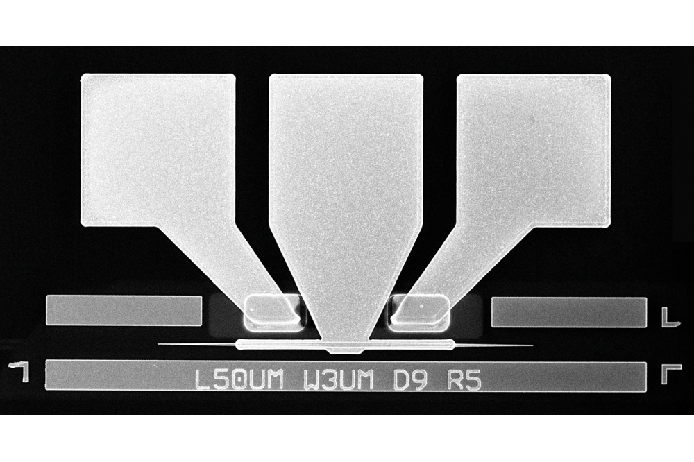
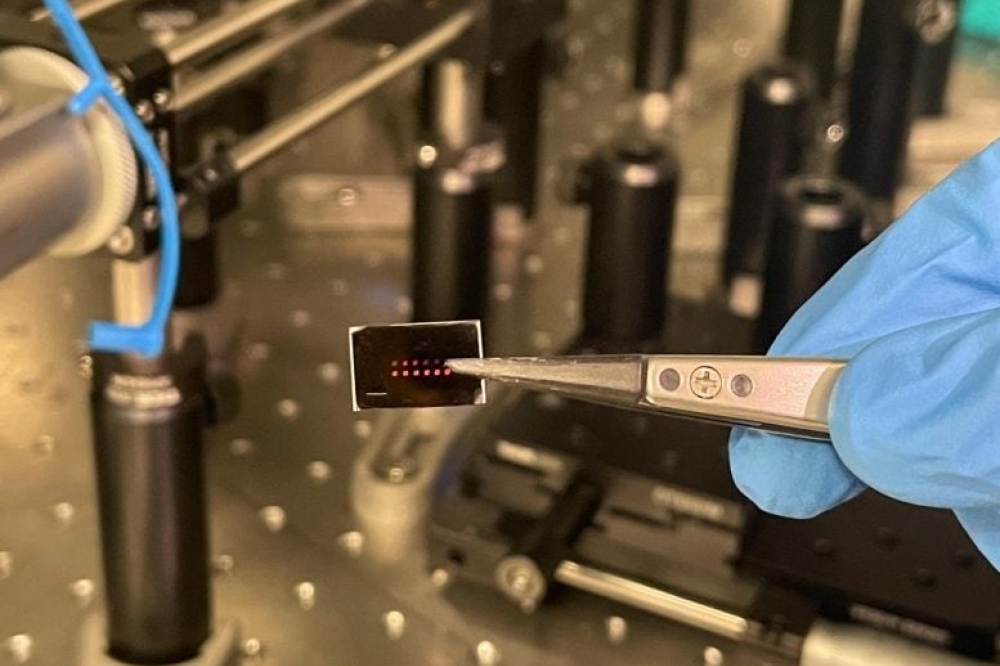
To achieve this, they embedded alignment marks made from concentric metalenses on the semiconductor chip. When light from a laser shines through these marks on both chips, it projects two interfering holograms. “This interference image shows if the chips are aligned or not, as well as the direction and the amount of their misalignment,” says Ghahremani.
“[Chip alignment] is a big, costly challenge for some of the companies that work in manufacturing semiconductor tools,” Arbabi says. “Our approach addresses one of the challenges of making them.” Lower costs also increase access to this technology for smaller start-up companies looking to innovate with semiconductors.
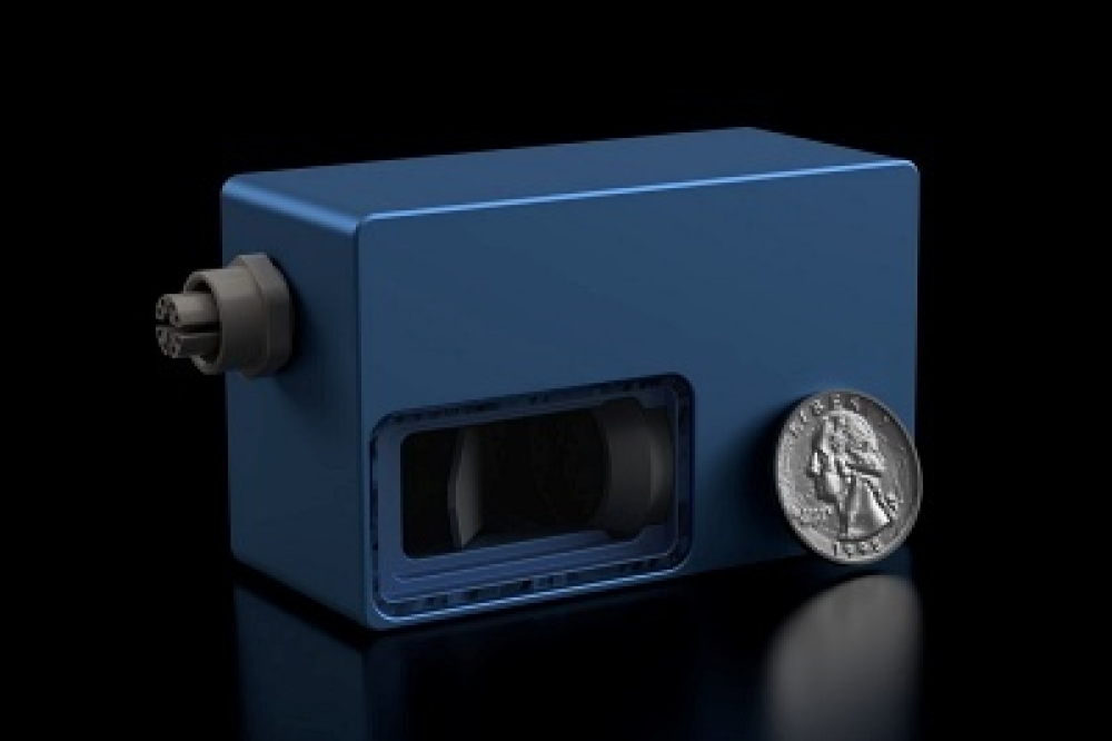
Arbabi also points out that this method can be used to make displacement sensors that can be used for measuring displacements and other quantities. “Many physical quantities that you want to detect can be translated to displacements, and the only thing you need is a simple laser and a camera,” he says. For instance, “if you want a pressure sensor, you could measure the movement of a membrane.” Anything that involves movement – vibration, heat, acceleration – can in theory be tracked by this method.


