FormFactor and Advantest collaborate on silicon photonics testing

The companies say their novel test cell and measurement system offers the world’s fastest automated photonic alignment, and equips photonics device developers with the tools to scale up volume production
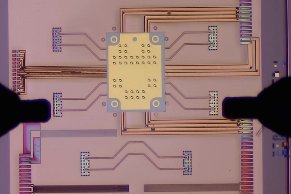
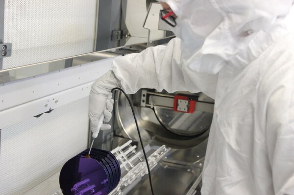
FormFactor, Inc. and Advantest Corporation have announced a strategic partnership to develop a novel test cell and measurement system designed for high-volume production of silicon photonics and co-packaged optics (CPO) devices. This collaboration is driven by the revolution in AI datacentre architectures, which require ever-increasing bandwidth while reducing power consumption.
Silicon photonics is rapidly gaining traction in datacentres for its ability to enable fast data transmission through optical signals, surpassing traditional electrical methods. According to FormFactor and Advantest, this new test cell integrates the latest innovations from both companies, equipping photonics device developers with the tools they need to scale up volume production.
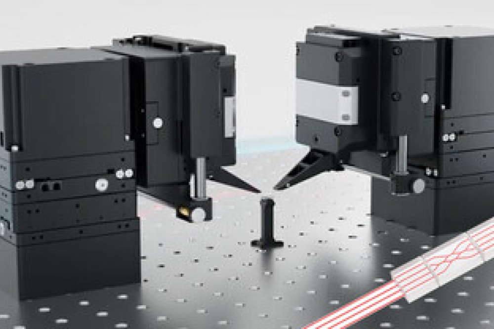
The companies say that the test cell offers the world’s fastest automated photonic alignment with nine-axis nano-precision, delivering significantly higher throughput compared to other technologies.
Among other benefits, FormFactor and Advantest say the system features wafer-level low-loss edge and surface coupling for photonic devices, with single-click automated calibration, as well as low coupling loss from the fibre to the device.
The companies add that the device combines with FormFactor’s Apollo probe architecture for production proven volume test of optical and electrical devices, and that it has a superior instrumentation set for HPC/AI/datacentre devices within a proven manufacturing environment.
Together, these and other capabilities aim to significantly shorten the time for opto-electrical testing and provide accurate, reliable measurements. According to FormFactor and Advantest, the platform now also facilitates optical measurements through seamless integration with essential equipment, such as laser sources, power meters, and optical signal routing and control instruments.
“The close collaboration between FormFactor and Advantest has resulted in one of the most automated, full-featured test and measurement systems available today for silicon photonics devices,” said Jens Klattenhoff, VP and GM of the Systems Business Unit at FormFactor. “By leveraging our expertise in calibration, motion technology, and rapid optical alignment, along with our joint advanced control software, we deliver high-precision, verifiable measurements immediately after system installation. FormFactor’s extensive experience in silicon photonics, including wafer and die-level probing, allows us to support our customers at every stage – from initial development to full-scale production.”
Juergen Serrer, senior executive officer and chief technology officer at Advantest, said: “As a global leader in automated test equipment for AI and high-performance computing, Advantest continues to drive innovation with the V93000 platform, now extending its capabilities to support silicon photonics and CPO devices. Innovations such as those featured in this new test system will deliver significant benefits to our customers.”


