Silicon-organic hybrid slot waveguide modulators on the verge of industrial adoption

Complementing highly scalable silicon photonics with engineered organic materials offers a path towards optical transceivers with unprecedented performance and efficiency. Recent data proves the photochemical stability of silicon-organic hybrid devices at practically relevant power levels, removing the last roadblock to industrial adoption.
BY Adrian Mertens, Carsten Eschenbaum, and Christian Koos AT SILORIX
Generative artificial intelligence (AI) is about to fundamentally transform our world, penetrating virtually every domain of modern life – from healthcare and diagnostics to industrial design and optimised production to stunningly realistic art, to name just a few. On a technical level, generative AI crucially relies on specific types of neural networks such as large language models (LLMs), which have tens of billions or even hundreds of billions of free parameters and which are designed to process and emulate human text or other content based on vast amounts of training data.
Training LLMs is a grand computational challenge, requiring massively parallel processing in dedicated AI clusters that contain thousands of highly specialised computing nodes, such as graphics processing units (GPUs) or tensor processing units (TPUs). However, scaling AI clusters – and hence the performance of associated LLMs – beyond current sizes is becoming increasingly difficult, primarily due to interconnect bottlenecks that limit the data transfer among the various computing nodes. Overcoming these bottlenecks is key to building even larger AI models that can take performance to yet another level.
Figure 1. Concept and performance of SilOriX’s silicon-organic hybrid
(SOH) technology, combining established silicon photonics with highly
efficient organic electro-optic (OEO) materials. (a) Basic concept of an
SOH Mach-Zehnder modulator (MZM). The device comprises a silicon
photonic slot waveguide in each arm, covered with an organic
electro-optic (OEO) material. Appropriate poling of the OEO material
leads to highly efficient chirp-free push-pull operation at ultra-low
∏-voltage length products UπL < 0.5 Vmm. Upper right:
Footprint of 8 x 200G = 1.6T transmitter blocks, implemented by SOH MZM
(left) and by standard pn-type silicon photonic MZM (right). (b)
Benchmarking of SOH slot waveguide modulators with respect to competing
technologies, in terms of efficiency & compactness and scalability.
SOH devices can rely on highly scalable silicon photonic base structures
that can be efficiently mass-produced, while the OEO material is
applied in wafer-level post-processing steps (see Figure 4).
In this context, it is widely accepted that massively parallel optical transmission will play an essential role, but current optical transceiver technology is still struggling to cope with the tough scalability and reliability challenges of AI clusters. In previous years, silicon photonics has emerged as a mainstay for cost-efficient mass production of optoelectronic devices and systems. However, conventional silicon photonic transceivers are fundamentally limited by the properties of silicon as the underlying functional material system. These limitations are becoming increasingly obvious in light of established and emerging transceiver standards with interface rates between 1.6T-12.8T [1]. One of the key requirements in optical transceiver technology is therefore to improve the performance scalability of silicon photonic transmitter circuits while maintaining their amenability to cost-efficient mass production.
Silicon-organic hybrid (SOH) slot-waveguide modulators
One of the primary limitations of conventional silicon photonics is the absence of Pockels-type optical nonlinearities – a direct consequence of the centrosymmetry of the silicon crystal lattice.
For this reason, conventional silicon-photonic modulators must rely on free-carrier injection and depletion via corresponding diode structures that are integrated into the waveguide core. This leads to comparatively low modulation efficiency, limited modulation speed, and unavoidable coupling of amplitude and phase modulation.
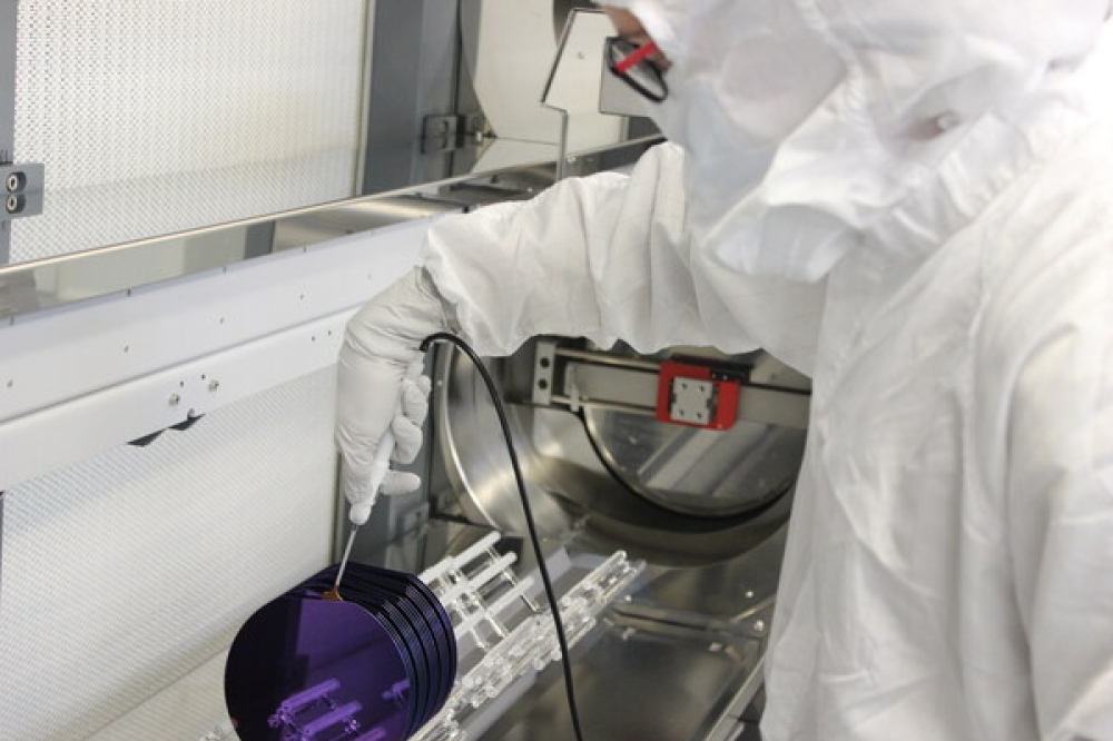
Figure 2. An 8-inch SOH wafer fabricated by SilOriX and its partners,
carrying more than 25,000 SOH modulators along with a wide range of
high-end silicon photonic circuits for various applications in optical
communications, ultra-broadband signal processing, and optical
metrology.
Silicon-organic hybrid (SOH) devices overcome these problems by combining silicon photonic waveguide structures with highly efficient organic electro-optic (OEO) materials, for which an ultra-high in-device Pockels coefficient of 390 pm/V has been obtained by theory-driven molecular design [2]. Figure 1(a) shows the basic concept of an SOH Mach-Zehnder modulator (MZM), where each arm contains a silicon photonic slot waveguide that is filled with the OEO material. The slot-waveguide structure increases the interaction between the guided light and the OEO cladding. The electrical signal is applied via a millimetre-wave transmission line, here illustrated in ground-signal-ground (GSG) configuration, which is connected to the doped rails of the slot via thin silicon slabs.
Appropriate poling of the OEO material allows for highly efficient chirp-free push-pull operation at ultra-low π-voltage length products, UπL < 0.5 Vmm. This leads to ultra-compact devices with sub-millimetre lengths that can be operated with drive signals of a few hundred millivolts peak-to-peak swing, thus paving a path towards efficient linear-drive operation by standard CMOS circuitry.
Figure 1(b) benchmarks SOH slot waveguide modulators with respect to competing technologies. SOH devices can rely on highly scalable silicon photonic base structures, which can be seamlessly co-integrated with the wealth of existing silicon photonic devices without any change to the front-end-of-line processes. The functional OEO cladding is then applied by efficient wafer-level post-processing without interfering with any front-end-of-line steps (see Figure 5). SOH technology is therefore amenable to cost-efficient mass production, just like conventional silicon photonics, while providing electro-optic modulators with ultra-low UπL products and hence record-high efficiency. Plasmonic-organic hybrid (POH) devices are subject to rather high optical losses and are therefore not included in Figure 1(c), despite having unparalleled modulation speed [3]. The upper right of Figure 1(a) also illustrates the compact footprint of SOH devices, even in direct comparison to conventional silicon photonic modulators, and emphasises the scalability and integration density of SOH devices once more. Figure 2 shows an 8-inch SOH wafer fabricated by SilOriX and its partners, carrying more than 25,000 SOH modulators along with a wide range of high-end silicon photonic circuits for various applications in optical communications, ultra-broadband signal processing, and optical metrology.
Figure 3. Long-term photostability test of SilOriX SOH MZM. By intimate
combination of material, process, and device development, SilOriX has
managed to eliminate stability problems in its SOH devices, that were
long perceived a roadblock towards industrial exploitation of the
technology. The devices under test were operated for more than 2500
hours at an on-chip power of 10 mW, without any sign of
photodegradation.
SOH processing and photochemical stability
A series of research demonstrations has proven the outstanding performance of SOH devices, but industrial adoption has so far been hindered by a lack of proven long-term stability of the underlying OEO materials [2]. The processes behind OEO degradation can be largely subdivided into two mechanisms. One mechanism is de-poling, i.e. the loss of preferential alignment of the functional OEO groups (“chromophores”), which is established in a one-time poling process during device fabrication. The other mechanism is photochemical degradation of the chromophores under high optical intensities. It has previously been demonstrated that the problem of de-poling can be overcome either by using materials with high glass-transition temperature [5], permitting long-term stability at 85 degrees Celsius, or by cross-linking of the organic matrix after poling [6], through which operation temperatures of 120 degrees Celsius can be reached.
In contrast, photochemical stability has continued to pose a challenge. However, there is another industry we can learn from. It turns out that the main mechanism responsible for photochemical degradation is just the same as the one that led to lifetime limitations of early-stage optical light-emitting diodes (OLEDs). This process involves optical excitation and the subsequent reaction of an organic chromophore with ambient oxygen, leading to a highly reactive singlet oxygen molecule, which can then chemically attack the functional group of the chromophore in a further reaction [7].
This insight points towards a solution: dedicated processing paths combined with appropriate device architectures and chip-level sealing techniques – just like in state-of-the-art OLED displays. Still, the extraordinarily high optical intensities in SOH devices represent a major problem. Specifically, the strong confinement of the guided light in the slot waveguide, which enhances the interaction with the OEO material, and which is key to the outstanding device efficiencies, unavoidably leads to large optical intensities in the slot region.
Figure 4. (a) 100 GBaud PAM-4 (200G) eye diagram of a packaged C-band
SOH modulator. (b) 192 GBaud PAM-4 (384G) eye diagram generated in an
O-band proof-of-concept experiment of SilOriX and its partners [4].
Assuming a wavelength of 1550 nm and an optical power of 10 mW propagating in a typical slot waveguide, the intensity in the slot region can easily reach values of the order of 5 MW/cm2, which corresponds to approximately 1000 times the optical intensity on the surface of the sun! Such high intensities do not occur in conventional PICs and are therefore not covered by current reliability standards and test protocols. This might also be the reason why previous stability tests of SOH devices have only been performed at comparatively low intensities of, for example, 500 kW/cm2 [8] – roughly an order of magnitude below the intensities that can be expected in practical applications.
Despite these immense challenges, SilOriX has overcome photodegradation of its SOH devices, through the joint development of materials, device architectures, and processing paths along with consequent testing at practically relevant intensity levels. This work has removed the last fundamental roadblock towards industrial exploitation of SOH technology.
Figure 3 shows the test data of a packaged C-band (λ = 1550 nm) device, operated with an on-chip power of 10 mW per slot waveguide. The vertical axis corresponds to the degradation factor p= Uπ (t)/Uπ (t=0), indicating the relative increase of the π-voltage Uπ over testing time t, relative to the beginning of the experiment (t = 0). The devices under test were operated for more than 2500 hours without showing any sign of photodegradation, thus paving the way for industrial application of long-term-stable SOH devices. We can infer the importance of the exact processing path from the strongly accelerated degradation of devices produced through non-optimised processes, indicated by the blue line in Figure 3.
What’s next?
Based on the demonstration of long-term-stable SOH devices (Figure 3), SilOriX is now establishing a dedicated SOH technology platform that builds upon a combination of proprietary device concepts, OEO materials, and processing workflows (Figure 5). Fundamental to this process chain is maintaining compatibility with wafer-level mass production, using, for instance, inkjet printing for material deposition and wafer-level testing for performance verification. Notably, OEO material deposition is exclusively done by post-processing and thus does not affect foundry-specific highly optimised silicon photonic fabrication processes.
Building upon this process chain, SilOriX is now starting to engage with industrial partners to transfer its SOH technology into commercial products. A major focus is on high-performance optical transceivers for intensity modulation and direct detection, which could be crucial for next-generation AI clusters. In this context, SilOriX is currently concentrating its efforts on transferring the technology from the telecommunication C-band (λ = 1530-1565 nm) and L-band (λ = 1565-1625 nm) to the O-band (λ = 1260-1360 nm), where chromatic dispersion is much less of an issue. SilOriX, together with Karlsruhe Institute of Technology (KIT), recently demonstrated the potential of SOH O-band modulators in a proof-of-concept experiment leading to a line rate of 384G transmitted by four-state pulse-amplitude modulation (PAM-4) in a single SOH-MZM (Figure 4(b)) [4]. This demonstration brings single-wavelength line rates of 400G or more within reach, which could greatly simplify the architectures of future 3.2T, 6.4T, or 12.8T Ethernet transceivers.
Figure 5. SilOriX’s SOH process chain. The SOH process starts with PIC
design and synthesis of dedicated organic electro-optic (OEO) materials.
After the fabrication of the PICs in commercial silicon photonic
foundries, the OEO materials are applied on wafer-scale via highly
efficient processes like inkjet printing, utilising industry-standard
equipment (e.g. the “n.jet semicon” by Notion Systems). The fully
functionalised SOH wafers are then characterised and diced. Known-good
SOH dies with outstanding performance can finally be integrated into
optical transceiver systems.
The voltage swing utilised for this transmission experiment was still below 1 Vpp, emphasising again the outstanding efficiency of SOH modulators. More specifically, SOH modulators can be driven directly with signals with sub-1 Vpp swing, which can be efficiently generated by CMOS circuits, thus significantly reducing the complexity and the power dissipation of the respective transceiver module. SilOriX has showcased this feature of their SOH modulators in live demonstrations at several conference exhibitions, for example, by driving a packaged MZM directly with the CMOS outputs of an industry-standard SerDes die, which provided 112G PAM-4 signals with 300 mVpp peak-to-peak swings [9]. By employing more sophisticated equipment and slightly higher swings, the SOH device demonstrated data rates of 200G PAM-4 (Figure 4(a)).
Note that the excellent performance of SOH modulators is not limited to intensity modulation and direct detection but can also be leveraged for coherent communications [2] – another interesting target application of SilOriX’s SOH technology. Moreover, SOH devices have recently been demonstrated to support cryogenic operation at temperatures of just a few Kelvin. Such devices might be instrumental to optical egress links that connect superconducting digital circuits or quantum processors at cryogenic temperature levels to their room-temperature environment [10].
Further application fields of ultra-efficient SOH phase shifters may emerge in the context of programmable photonics, ultra-broadband signal processing, or optical metrology and sensing. Just as happened with OLEDs in the past, we believe that SOH technology is now on the verge of entering industrial applications with tremendous potential, after having kept a low profile in academic research for over a decade.


