Quantum-dot lasers on silicon
Integrating quantum-dot lasers on silicon photonic
chips promises to create high-speed devices for datacom and other
applications.
BY ARTEM PROKOSHIN AND YATING WAN FROM KING ABDULLAH UNIVERSITY OF SCIENCE AND TECHNOLOGY
Since its invention in 1962, the semiconductor laser has played a phenomenal role in changing our world. This source of monochromatic emission is now an essential component in CD and DVD players and recorders, laser printers, barcode readers, and most importantly, fibre-optic communication systems that connect our world through the internet.
Internet traffic continues to climb at an eye-watering pace, with analysts calculating a compound annual growth rate of 25 percent that, in 2022, propelled global traffic to 4.8 zettabytes – that’s 4.8 trillion gigabytes. Given this tremendous rise in internet traffic, which shows no sign of abating, it is more important than ever to trim the power consumption of data transmitters and receivers. Efforts that are underway in that regard are not restricted to long-haul optical communications, and are also considering short-distance interconnects in datacentres, which now account for up to 2 percent of global electricity. The target is to drop below 1 picojoule per bit.
Fulfilling this goal will have far-reaching benefits. As well as helping to curb the carbon footprint in the datacom and telecom sectors, energy savings will help where there is a booming interest in the use of photonic chips in neural networks, known as photonic neural networks. With growing popularity of large language models, the cost of training and operating them is increasing. Photonic neural networks, driven by highly efficient semiconductor lasers, offer a promising solution to meeting this growing energy demand.
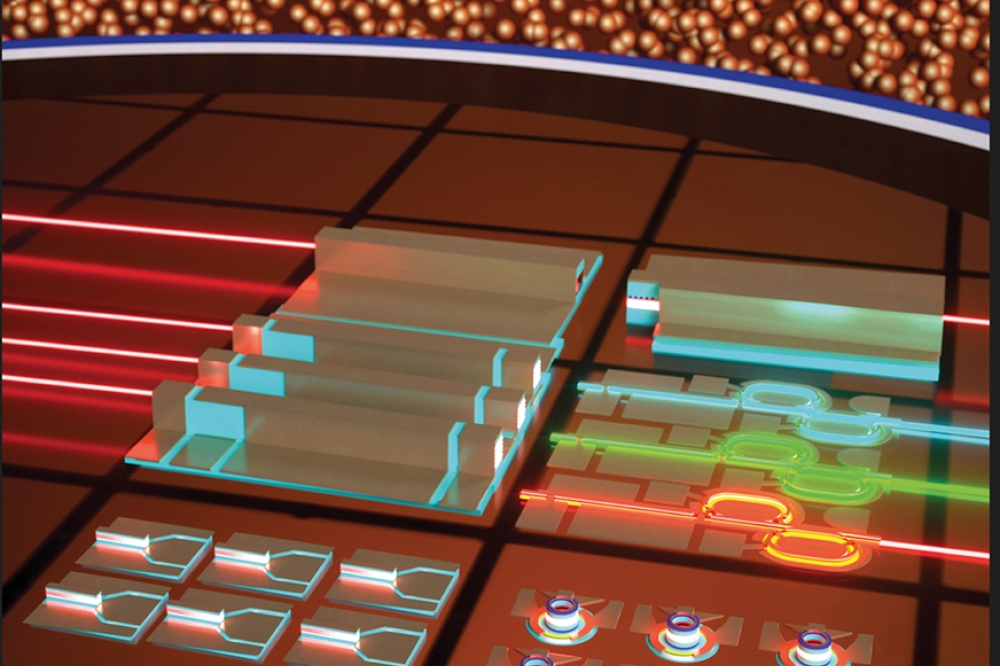
Helping to turn such dreams into reality by integrating quantum-dot lasers on silicon photonic chips is our team at the King Abdullah University of Science and Technology. By marrying these two technologies, we are uniting incredibly efficient sources with mature, high-volume semiconductor processing techniques.
Figure 1. The fabrication process for quantum-dot lasers on silicon.
Why silicon?
Silicon, by far the most widely used semiconductor material since the latter half of the last century, is the backbone of the microelectronics industry. When used to produce integrated photonics, silicon provides the most advanced material platform, developed over the last 20 years and relying heavily on CMOS technology. Merits of the silicon photonics platform include: a high refractive index contrast, leading to low-loss; high-confinement waveguides; and efficient grating couplers.
Drawing on silicon’s doping technology, chipmakers can produce high-speed modulators based on p-n junctions, while this material’s compatibility with germanium ensures fast and efficient silicon-germanium photodetectors. What’s more, silicon photonics provides the highest manufacturing volume and the lowest cost, thanks to the opportunity to manufacture silicon chips on 300 mm wafers.
Unfortunately, despite all these strengths, silicon is not the perfect choice. Its biggest disadvantage for photonic applications is its indirect bandgap, preventing it from providing an efficient light source. While several silicon-germanium laser diodes have been demonstrated, they are unsuitable for real-world applications, due to their feeble output power and broad linewidth.
The lack of a silicon-based laser has led to the pursuit of two options for producing PICs with this material system. One involves combing silicon photonic chips, as purely passive devices, with an external light source. In this case, the downsides are high coupling losses, typically exceeding 3 dB, and increased packaging complexity. The second option is to integrate efficient lasers based on III-V semiconductors, such as GaAs or InP, directly onto silicon photonic chips. This approach reduces coupling loss to typically below 0.5 dB and simplifies packaging, but leads to constrained production volumes and increased costs.
Why quantum dots?
Since the introduction of the first semiconductor lasers, there have been a number of improvements to their design, along with the development of various different architectures. The first lasers were homojunction diodes, using the same material for the waveguide core material and its surroundings. To improve optical confinement, a breakthrough that ensured the first continuous-wave operation, engineers introduced a double heterostructure, sandwiching the active region between a pair of cladding layers with a wider bandgap and a lower refractive index. For example, this has been realised by surrounding a GaAs active region with AlGaAs. Another important advance followed, with a move to an active region employing a multiple quantum well structure that improves the efficiency of the radiative recombination process.
The next logical step, pursued by many in recent decades, is a move from a multi-quantum-well active region to one based on quantum dots. With this refinement, carrier confinement switches from one lateral direction to all three dimensions. Quantum dots, also referred to as ‘zero-dimensional’ structures, have dimensions on the order of tens of nanometres. They can be formed with a self-assembly process, involving epitaxial growth of InAs on a lattice-mismatched GaAs substrate.
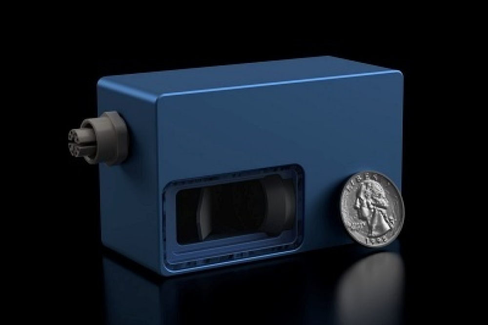
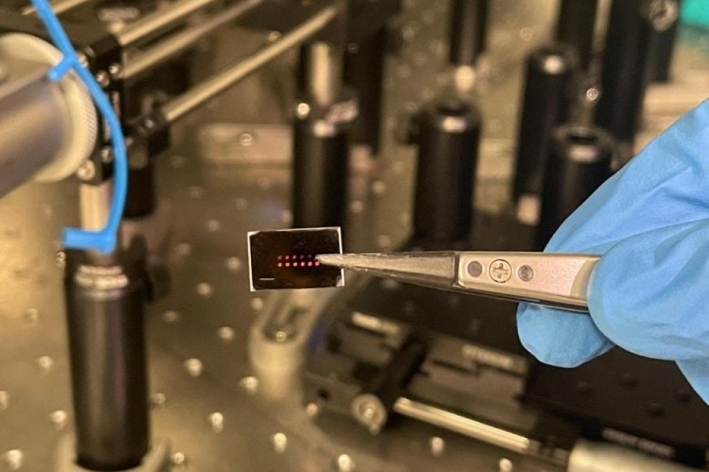
Figure 2. (a) QD laser mounted in a butterfly package. (b) Frequency
noise spectra of QD lasers with a 1 mm and 1.5 mm long cavity. The
linewidth in the free-running regime is 41 kHz. (c) Illustration of the
coupled compound cavity. (h) and (i) Measured and calculated frequency
noise spectra, indicating a fundamental linewidth of 16 Hz.
The father of the quantum dot laser is Yasuhiko Arakawa from the University of Tokyo. In 1982 he proposed this device, claiming it had the potential to provide a lower threshold current and better temperature stability than its quantum-well-based cousins. Thanks to an atom-like structure and a discrete density of states, the quantum-dot laser provides an almost symmetric gain spectrum and a low linewidth enhancement factor, enabling narrow-linewidth and isolator-free operation. Additional opportunities for quantum dots are found in low-dark-current photodetectors and efficient Stark-effect amplitude modulators.
In the context of integration with silicon, the main advantage of quantum dots is a reduced sensitivity to crystal defects. These nanostructures offer improved in-plane carrier confinement, with diffusion lengths on the order of several microns – that compares with tens of microns in quantum wells, and ensures that dots are highly tolerant to dislocation defects.
The great potential of quantum dots is realised in devices. Measurements of quantum-dot lasers demonstrate that they can operate with a long extrapolated-lifetime at high temperatures, thus relaxing the stringent requirements on temperature control of photonic chips. This class of laser also offers a threshold current of less than 1 mA, making it an ideal candidate for addressing the ever-increasing energy consumption in optical communication networks.
Combining the two
When quantum dot lasers are integrated with silicon photonics, rather than being manufactured on native substrates, both improvements and drawbacks result. Focusing on the positives, there is the integration of quantum-dot active regions with high-quality grating structures and ring resonators to realise single-mode lasing. In addition, there is a lower propagation loss for silicon waveguides compared with III-V materials – this leads to lower threshold currents and a narrower linewidth for integrated lasers with an extended cavity.
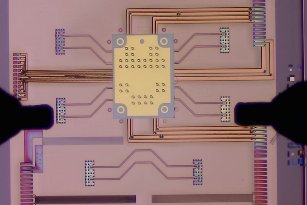
Recently, we have directed our efforts at the heterogeneous integration of quantum-dot lasers on silicon via wafer bonding. This has involved the use of silicon-on-insulator substrates with a 500 nm-thick layer of silicon, which provides higher mode overlaps between the silicon and quantum-dot regions compared with the standard, 220 nm-thick silicon photonics platform.
Production of our PICs began with patterning our SOI wafer with three different etching depths: a 500 nm etch for strip waveguides, a 231 nm etch for rib waveguides, and a 20 nm etch for grating structures. Following this patterning process, we bonded our GaAs wafer to the quantum-dot active region, prior to annealing at 100 °C and removing
the GaAs substrate. GaAs mesas were then patterned to form laser active regions, followed by the deposition of the contact metal layer (see Figure 1 for a step-by-step illustration of the entire fabrication process).
With this approach, light generated in the quantum-dot active region is directed into the silicon waveguides by evanescent coupling. This occurs when two waveguides are close to each other – typically less than the wavelength of the light – a situation that allows light to transfer from one waveguide to another (see Figure 2). To increase coupling efficiency and cut back-reflections, we employ a
taper rather than an abrupt transition between the III-V and the silicon waveguide. By terminating the silicon waveguide at the end of the chip with a 7 ° angled taper, we reduce back-reflection at the facets.
Our lasers achieve single-mode operation with a side-mode suppression ratio of over 60 dB (see Figure 3 (a)) and a threshold current of just 4 mA. The latter corresponds to a threshold current density of 31 A cm-2, which is an order of magnitude lower than that of standard quantum-well lasers.
These directly modulated quantum-dot lasers are attractive candidates for datacentre communications, as they do not require additional modulators based on silicon or lithium niobate. However, due to a finite intraband relaxation time and gain saturation effects, it’s a challenge to realise a high modulation bandwidth with quantum-dot lasers, with the 3 dB modulation frequency typically limited to around 10 GHz for devices grown on native substrates. However, thanks to synergistic effects between the silicon cavity and the quantum-dot active region, our heterogeneous quantum-dot device produces a modulation frequency of 13 GHz at an injection current of 31 mA (see Figure 3 (c)) for the corresponding small-signal response).
Another important characteristic for lasers used in optical communications is their linewidth, which indicates the noise level and ultimately limits data transmission capacity. QD lasers have a low linewidth enhancement factor, leading to narrower linewidths than the quantum-well counterparts. Early collaborative efforts have also spotlighted the unique properties of QD lasers in chaos-free operation, achieving a remarkably low 16 Hz Lorentzian linewidth under external-cavity locking with a low-Q cavity – an improvement in frequency noise by an order of magnitude over conventional quantum-well lasers. Standalone, these QD lasers (see Figure 2 (a)) exhibit a 41 kHz linewidth (see Figure 2 (b)). Under external optical feedback, a 35 dB improvement in feedback insensitivity has been achieved, enhancing stability and enabling operation without coherence collapse even with -9.6 dB of feedback. This makes the QD lasers suitable for integration into compact, highly integrated photonic systems without the need for optical isolators.
Looking ahead, there is theoretical potential for an even more dramatic reduction in linewidth – to 1 Hz or less – by employing a high-Q silicon-nitride--based micro-ring resonator in conjunction with the self-injection locking technique, as shown in Figure 2 (d) and (e). This prospective development is particularly suited for microwave photonics applications, including microwave synthesisers where stability is paramount.
Outstanding challenges
It is beyond question that quantum-dot lasers on silicon are a promising solution to addressing the growing energy demand in datacentre optical communications. These sources are markedly superior to their quantum-well counterparts in key performance criteria, including threshold current, linewidth and temperature stability. Additional merits of these lasers are a high output power and an exceptional modulation frequency.
Still, there is considerable work to do to make this technology viable and affordable in high-volume production. Efforts must be directed at realising wafer-scale integration on 300 mm substrates to fully exploit the high-volume, low-cost production capabilities of silicon photonics. Other outstanding goals are to integrate quantum-dot lasers with high-speed silicon modulators and photodetectors, and to undertake a systematic study of reliability with high-power testing, to prove that quantum-dot lasers can deliver reliable operation at the elevated temperatures found in data centres. Once these tasks have been accomplished, the next step will be to demonstrate a platform that is best at leveraging the economies-of-scale of silicon while maintaining the highest yield at the lowest lifecycle cost.
The capability of our technology allows its opportunities to stretch beyond datacentres. The realisation of the dense integration of devices with on-chip lasers is an advance that will prove crucial in many of tomorrow’s applications, including photonic neural networks, biochemical sensing and quantum computing. The addition of on-chip laser sources enables all-optical signals to be confined within an integrated circuit package, enhancing efficiency, stability, and scalability. This integration is poised to revolutionise many applications, while offering significant performance improvements, environmentally friendly solutions, and the potential for mass production.


