Nanoscribe wins ECOC 2024 award for Quantum X align

The company says its product, which won most innovative product in the chip-scale packaging/optical sub-assembly category, enables printing of low-loss optical couplers that are automatically aligned to photonic chips or optical fibres
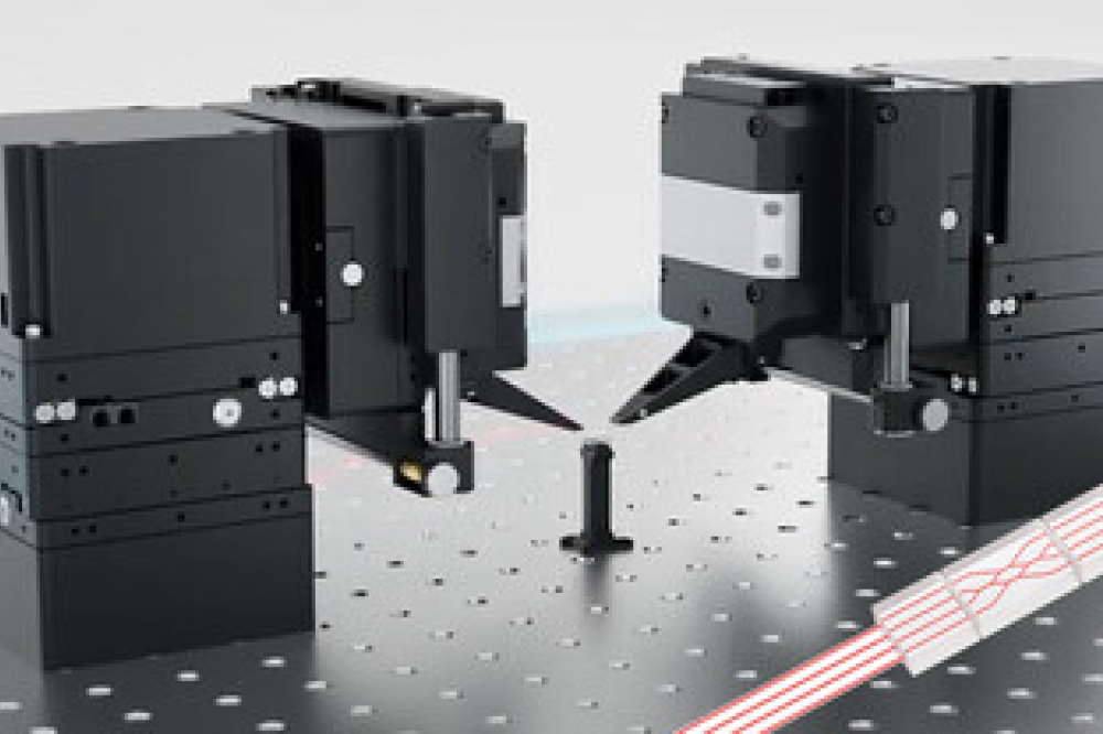
Nanoscribe has received the ECOC Industry Award for its Quantum X align high-resolution 3D printer as the most innovative product in the “Chip-Scale Packaging / Optical Sub-Assembly” category. Jan Szabados, product manager at Nanoscribe, accepted the award at the ECOC 2024 exhibition in Frankfurt, Germany. The Quantum X align aims to enable printing of low-loss optical couplers that are automatically aligned to fiducials on various types of photonic chips or optical fibres.
“This is a huge recognition of the transformative potential of the Quantum X align,” said Szabados. “More than anything, this award is a testament to our team's dedication to build a product that truly addresses one of the main challenges of today’s photonic integration landscape: low-loss, high-reliability optical coupling between different optical components.”
The large number of different substrates and interfaces used in the photonic integration market calls for versatile low-loss optical couplers that can connect different material platforms with their specific optical characteristics such as mode fields. According to Nanoscribe, Quantum X align addresses these market needs by enabling 3D printing of freeform micro-optical elements aligned to fiducials, such as waveguides, markers on photonic chips, or chip edges. The company says that the accuracy of the lateral alignment reaches down to 100 nm, and the suitable material platforms are almost unlimited, allowing printing on silicon, silicon phosphide, silicon nitride, silicon on insulator, indium phosphide, lithium niobate, glass, and more. In this way, Nanoscribe aims to advance photonics packaging by providing aligned 3D printing of optical interconnects without the need for further assembly, active alignment or fixation steps.
For photonics applications, it is crucial to have micro-optical elements with the best possible shape accuracy, optical surface quality, and accurate placement and alignment to the structures to be interconnected. Nanoscribe says that, with its proprietary Aligned 2-Photon Lithography (A2PL) technology, all types of freeform micro-optics can be printed directly onto optical fibre tips, photonic chip edges, chip surfaces or wafers, always spatially aligned to fiducials and 3D topographies, resulting in robust optical interconnects with minimal optical attenuation, even in cryogenic environments.
However, industrial scale manufacturing is not only about quality, but also about throughput. Nanoscribe has therefore extended its Two-Photon Grayscale Lithography (2GL) technology to the third dimension. The so-called 3D printing by 2GL, is based on dynamic voxel tuning that Nanoscribe says requires significantly fewer printing layers to achieve outstanding printing results in the shortest possible time. According to the company, throughput is increased by up to 60 times while maintaining the highest level of shape accuracy and optical surface quality.


