Sivers plans photonics spin-off

Sivers Semiconductors AB has entered into a non-binding letter of intent to merge its Sivers Photonics Ltd subsidiary with byNordic Acquisition Corporation, a publicly-traded special purpose acquisition company.
The merger is expected to unlock significant value and create an independent US NASDAQ traded photonics company. (Sivers Photonics currently has approximately 80 percent of its net revenue in the US).
Sivers today consists of two subsidiaries addressing two different markets: Wireless and Photonics.
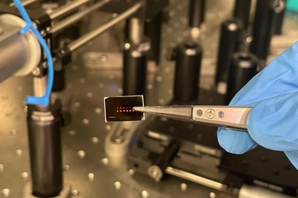
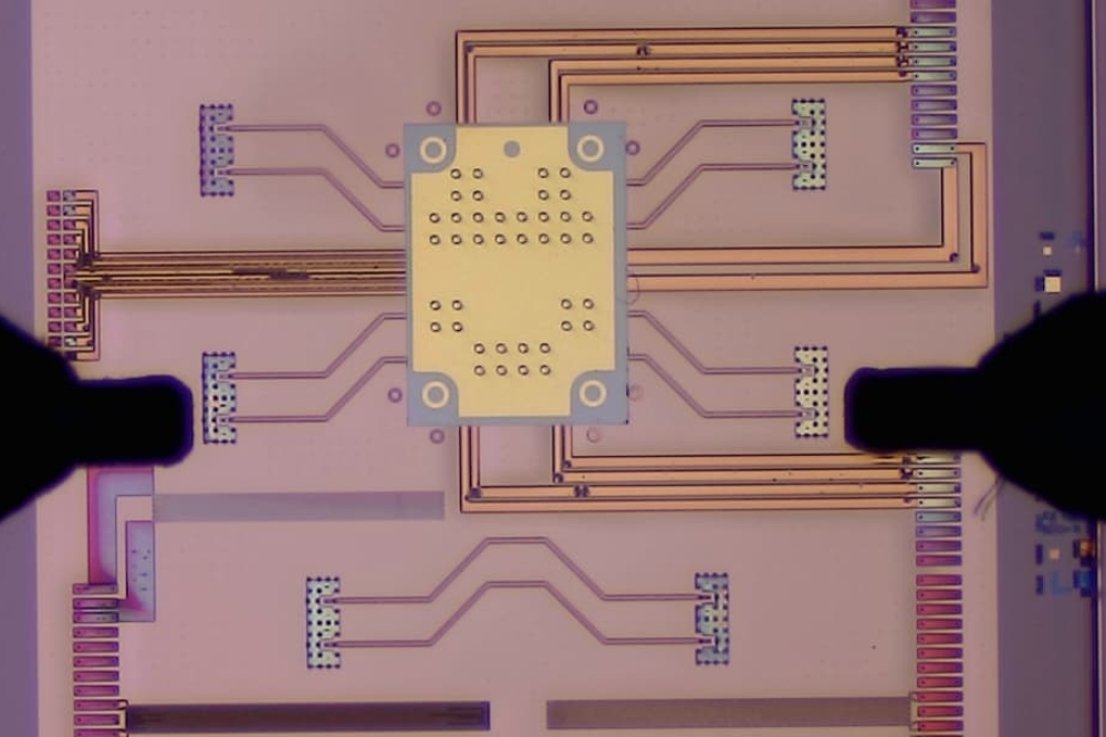
The Sivers’ Photonics subsidiary has particular focus on InP technology, with which it develops customisable lasers aimed at high-growth AI infrastructure and sensing applications for data centres, consumer healthcare and automotive LIDAR. The company has three issued patents and 16 patents pending across the US, UK, Canada and the World Intellectual Property Organisation.
Additionally, Sivers Photonics has development contracts to develop unique lasers for several leading silicon photonics providers, such as Ayar Labs, and is in discussion with several leading AI companies, including hyperscalers.
Subsequent to the proposed spin-off and Sivers Photonics merger combination, Sivers' remaining wireless business will consist of a portfolio of products in mmWave beamformer front-end integrated circuits, RF transceivers, repeaters, and software algorithms for mmWave RF performance for satellite and 5G Infrastructure. Wireless business net revenue growth was 155 percent in 2023, reaching approximately $15 million. These markets are developing rapidly, and Sivers has secured a number of contracts and design wins that are projected to drive significant product revenue growth over the next 3-5 years.
“We believe the potential for AI Photonics is immense yet overshadowed by the equally exciting Sivers´ Wireless business unit. With the attractive opportunity for silicon photonics in AI infrastructure and the emerging demand for photonic biometric sensors, we feel now is the right time to shine a light on this business unit as a standalone entity to gain access to the US capital markets and create an opportunity for our shareholders to participate in its potential future success,” said Bami Bastani, Sivers Semiconductor chairman.
“At the same time, we also look to capitalise on the success of the Sivers’ Wireless business unit and the demand for our leading-edge mmWave beamformer solutions for satellite and 5G, which has gained substantial traction with customers in these developing markets over the last several years, enabling us to create a fully fabless and less capital-intensive company that will remain listed under Sivers Semiconductors AB.”


