
Nanostructures’ light emission patterns revealed using 3D printing method
Researchers report highly directional light emission from 3D-printed nanowires, and say that their work could benefit fields that use ultra-small light-emitting materials, including integrated photonics
Researchers at the Korea Electrotechnology Research Institute (KERI) have reported revealing light emission patterns from 3D-printed nanowires for the first time. Their work has been published as a cover article in the scientific journal ACS Nano.
In the pursuit of higher pixel density, offering higher-resolution image displays, efforts are being made to fabricate smaller and smaller light-emitting devices, from the micrometre scale (one millionth of a metre) to the nanometre scale (one billionth of a metre).
However, as the size of light-emitting devices shrinks to hundreds of nanometres, peculiar changes occur in the light-matter interaction, resulting in significantly different emission patterns compared to macroscale structures. Therefore, understanding the light emission from nanostructures is an essential prerequisite for the practical application of nanoscale light-emitting devices.
The KERI research team, led by Jaeyeon Pyo, report that, by using nanophotonic 3D printing technology, they have revealed highly directional light emission patterns from 3D-printed nanowires.
Nanophotonic 3D printing technology is a technique for implementing photonic devices using a nanoscale high-resolution 3D printing method. Fabrication of nanoscale photonic structures in 3D architecture is achieved by direct writing of functional inks formulated from various optical materials. This technology is expected to bring innovation to ultra-high-resolution displays, security printing, data storage, and more.
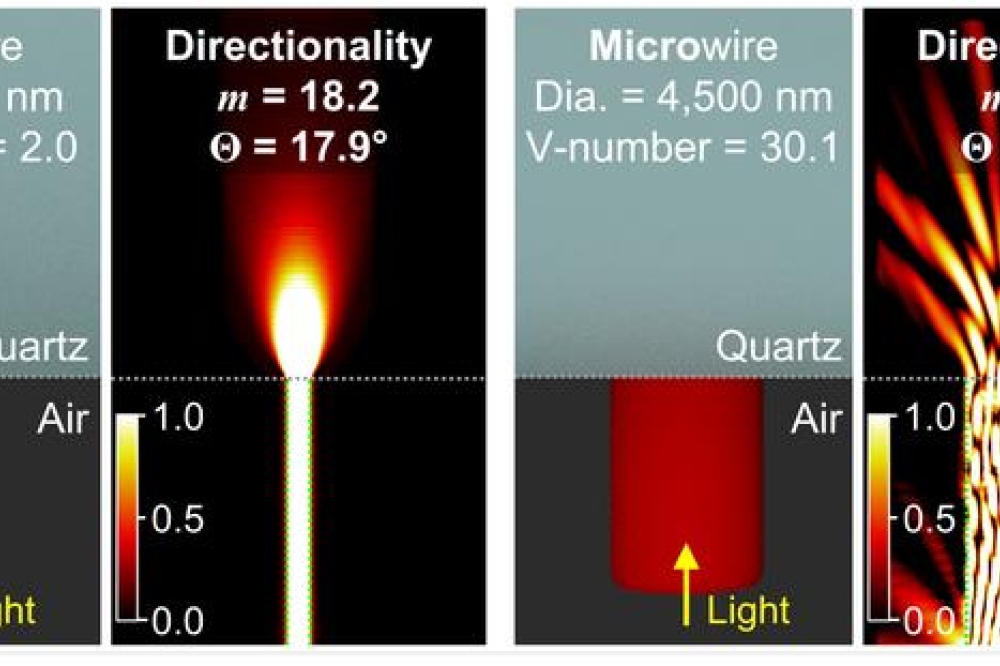
Typically, it is challenging to uniformly fabricate light-emitting materials of desired sizes at specific locations using conventional chemical or physical vapour deposition methods. However, according to the scientists, KERI’s 3D printing technology allows precise control of the diameter through the restriction of the printing nozzle’s aperture, enabling the reliable fabrication of light-emitting materials at desired locations with a wide range of sizes (ranging from one ten thousandth of a metre to one tenth of a millionth of a metre).
Pyo’s team experimentally observed and measured light emission patterns from specimens precisely fabricated using the nanophotonic 3D printing technology, ranging in size from the nanometre to micrometre scale. The team also conducted electromagnetic wave simulations for in-depth analysis and cross-validation of their arguments.
As a result, when the size of light-emitting materials becomes as small as 300 nanometres in diameter, internal reflection of light vanishes due to spatial confinement, leading to one-directional straight propagation of light. Consequently, the light emission pattern becomes highly directional. Typically, light propagates through diverse paths within a given internal structure, resulting in broad emission patterns due to their superposition. However, in nanowire structures, only a single path exists, leading to the observed highly directional emission pattern.
According to the scientists, this observed high directionality can significantly enhance the performance of displays, optical storage media, encryption devices, and more. Macro-structures with broad emission patterns can suffer from optical crosstalk when densely integrated, causing signals to overlap or blur. In contrast, the researchers say that nanowires with highly directional emission patterns allow clear separation between signals from each structure at high densities, eliminating distortions in representation or interpretation. The highly directional emission of nanowires makes them suitable for high-performance devices, as experimentally demonstrated by KERI’s team.
“Research on optical physics at the nanoscale is challenging, especially due to the difficulty in specimen preparation, which is often high-cost and time-consuming,” said Pyo. “Our contribution demonstrates that the 3D printing method can be a versatile platform for studying optical physics owing to its simple, flexible, and low-cost characteristics. This research will significantly contribute to the cutting-edge display technologies, and quantum physics, which are part of South Korea’s ‘National Strategic Technology Nurture Plan.’”
The research team anticipates that their contribution will attract significant interest in the fields of virtual reality (AR, VR), beam projectors, optical storage media, PICs, encryption technologies, and security printing, where ultra-small light-emitting materials can be utilised. They aim to continue investigating various optical phenomena occurring at the nanoscale using the 3D printing method, leveraging its capability for free-form fabrication.
Image credit: Korea Electrotechnology Research Institute (KERI)


