
High-performance erbium-doped waveguide laser on silicon nitride PIC
Researchers say they have built a laser that combines wavelength tuneability with practical photonic integration, and that it could be valuable in applications including gyroscopes and LiDAR
Lasers have revolutionised the world since the 1960s and are now indispensable in modern applications, from cutting-edge surgery and precise manufacturing to data transmission across optical fibres.
An important type of lasers are fibre lasers, which use an optical fibre doped with rare-earth elements (such as erbium, ytterbium, and neodymium) as their optical gain source (the part that produces the laser’s light). As well as emitting high-quality beams and having high power output, they are efficient, low-maintenance, durable, and typically smaller than gas lasers. Fibre lasers are also the gold standard for low phase noise, meaning that their beams remain stable over time.
Today, there is a growing demand for miniaturising fibre lasers down to a chip-scale level. Erbium-based fibre lasers are especially interesting, as they meet all the requirements for maintaining a laser’s high coherence and stability. But scientists trying to miniaturise them have encountered challenges in maintaining their performance at small scales.
Now, researchers led by Yang Liu and Tobias Kippenberg at EPFL say they have built the first-ever chip-integrated erbium-doped waveguide laser that approaches the performance of fibre-based lasers, combining wide wavelength tuneability with the practicality of chip-scale photonic integration. Their results are published in Nature Photonics.
Building a chip-scale laser
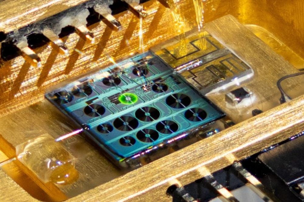
To develop their chip-scale erbium laser, the team began by constructing a metre-long, on-chip optical cavity (a set of mirrors that provide optical feedback) based on an ultra-low-loss silicon nitride PIC.
“We were able to design the laser cavity to be metre-scale in length despite the compact chip size, thanks to the integration of these microring resonators that effectively extend the optical path without physically enlarging the device,” says Liu.
The team then implanted the circuit with high-concentration erbium ions to selectively create the active gain medium necessary for lasing. Finally, they integrated the circuit with a III-V semiconductor pump laser to excite the erbium ions to enable them to emit light and produce the laser beam.
Aiming to refine the laser’s performance and achieve precise wavelength control, the researchers engineered an intra-cavity design featuring microring-based Vernier filters, a type of optical filter that can select specific frequencies of light. The filters are intended to allow for dynamic tuning of the laser's wavelength over a broad range, making it versatile and usable in various applications.
According to the team, this design supports stable, single-mode lasing with a narrow intrinsic linewidth of just 50 Hz, as well as allowing for significant side mode suppression – the laser’s ability to emit light at a single, consistent frequency while minimising the intensity of other frequencies (side modes). This results in a “clean” and stable output across the light spectrum for high-precision applications.
Power, precision, stability, and low noise
The researchers say their chip-scale erbium-based fibre laser features output power exceeding 10 mW and a side mode suppression ratio greater than 70 dB, outperforming many conventional systems. They add that it also has a very narrow linewidth, meaning the light it emits is very pure and steady, which is important for coherent applications such as sensing, gyroscopes, LiDAR, and optical frequency metrology.
According to the scientists, the microring-based Vernier filter gives the laser broad wavelength tuneability across 40 nm within the C- and L-bands (ranges of wavelengths used in telecommunications), surpassing legacy fibre lasers in both tuning and low spectral spurs metrics (“spurs” are unwanted frequencies), while remaining compatible with current semiconductor manufacturing processes.
Next-generation lasers
Miniaturising and integrating erbium fibre lasers into chip-scale devices can reduce their overall costs, making them accessible for portable and highly integrated systems across telecommunications, medical diagnostics, and consumer electronics.
It can also scale down optical technologies in various other applications, such as LiDAR, microwave photonics, optical frequency synthesis, and free-space communications.
“The application areas of such a new class of erbium-doped integrated lasers are virtually unlimited,” says Liu.
Image credit: Andrea Bancora and Yang Liu (EPFL)


