
Imec demonstrates progress towards die- and wafer-level optical interconnects
The institute is developing a process flow for direct die-to-wafer hybrid bonding for both copper and silicon carbon nitride, and has presented a copper bond pad pitch of just 2 µm
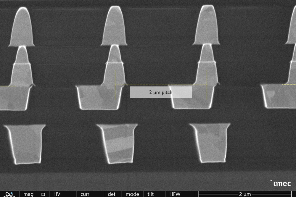
Last week, at the 2024 IEEE Electronic Components and Technology Conference (ECTC), the Belgian research institute imec presented a copper-to-copper and silicon carbon nitride-to-silicon carbon nitride die-to-wafer bonding process, which it says results in a copper bond pad pitch of only 2 µm at < 350 nm die-to-wafer overlay error, achieving good electrical yield. According to the institute, such fine-grained die-to-wafer interconnects pave the way to logic/memory-on-logic and memory-on-memory applications. In the longer term, imec says the die-to-wafer bonding will also enable die- and wafer-level optical interconnects – for which it demonstrated a first proof of concept at ECTC2024.
Imec is developing a process flow for direct die-to-wafer hybrid bonding at interconnect pad pitches well below 10 µm, down to 1 µm. To reach these goals, the institute says it achieved a major process improvement, in particular preserving ultraclean surfaces during processing, die singulation and pick-and-place, and maintaining a high throughput during all the process steps. This led to the demonstration with a copper bond pad pitch scaling down to 2 µm.
Hybrid bonding requires very high-quality surface preparation to achieve smooth surfaces with minimal copper pad recess (< 2.5 nm), requiring careful optimisation of the chemical-mechanical polishing (CMP) step of the copper or silicon carbon nitride surface. These properties need to be maintained during wafer singulation and die-to-wafer placement.
To achieve a high-quality die singulation, without particles and impact to the copper/silicon carbon nitride surface, imec says it implemented a plasma dicing process. Critical to the pad pitch scaling is a fast but high-accuracy pick-and-place step. The institute says that the die processing together with a high-accuracy pick-and-place step resulted in < 350 nm die-to-wafer overlay errors. The assembly flow enabled 2 µm pitch copper bond pads with good electrical yield: Kelvin e-yield > 85 percent and daisy chain e-yield > 70 percent.
Eric Beyne, senior fellow, vice president of R&D, and programme director of 3D system integration at imec, said: “In terms of interconnect pitch, die-to-wafer hybrid bonding can now bridge the gap between solder-based die-to-wafer bonding (which is likely to stagnate at 10 to 5 µm bump pitch) and wafer-to-wafer hybrid bonding (allowing interconnects well below 1 µm, down to 400 nm pitch (as presented at IEDM 2023), and possibly 200 nm pitch in the future). Compared to the latter, die-to-wafer bonding offers the advantage of stacking only known-good dies (resulting in higher compound yields) and of bonding dies of unequal size. Future improvements to our process flow will further push the interconnect pitch towards 1 µm. With this evolution, die-to-wafer bonding can enter the realm of memory/logic-on-logic and memory-on-memory stacking.”
In addition, high-precision die-to-wafer bonding processes are a key enabler for wafer-level optical interconnects – imec’s long-term vision for high-bandwidth, low-power connections between multiple compute chips (xPUs) and high-bandwidth memory (HBM) in AI/ML clusters. An attractive approach from cost and yield perspective is to partition the optical interconnect in a passive optical interconnect wafer, containing long-range routing waveguides and passive optical functions, and active PIC dies (with modulators and photodetectors) – which in turn are bonded to an electrical IC (xPU or HBM).
Joris Van Campenhout, fellow and R&D programme director at imec, added: “As a first proof of concept, we enabled low-loss evanescent optical coupling between PIC dies and a 300 mm bottom optical interconnect wafer – leveraging a (collective) silicon carbon nitride dielectric-based die-to-wafer assembly process. Benefitting from the accurate die-to-wafer alignment, low optical coupling losses of below 0.5 dB were obtained. In the next steps, we will expand our assembly flow – e.g. by also providing copper-to-copper interconnects throughout the die-to-wafer stack.”
Image credit: imec


